Soft and hard boards have many benefits, many designers have not known before, because their design does not have to use this technology. However, more and more designers are now facing the pressure to build increasingly high-density electronic devices, and the headache is to continuously reduce manufacturing costs and manufacturing time. In fact, this is really not a new technical problem. Many engineers and designers have been headaches for a long time, and the pressure is increasing.
Therefore, it is wise to understand how to make flexible circuits and soft and hard boards. In this way, we can easily find the hidden dangers in the design and prevent it from happening. Now let us know what basic materials are needed to make these boards.
Flexible circuit material
Substrate and protective film
First, let's consider ordinary rigid printed circuit boards whose base materials are usually fiberglass and epoxy. In fact, these materials are a kind of fiber, although we call it "rigid", if you take a single layer, you can feel its elasticity. Because of the cured epoxy resin, the layer can be made more rigid. Because it is not flexible enough, it cannot be applied to some products. However, it is suitable for many electronic products that are simply assembled and that do not continuously move the board.
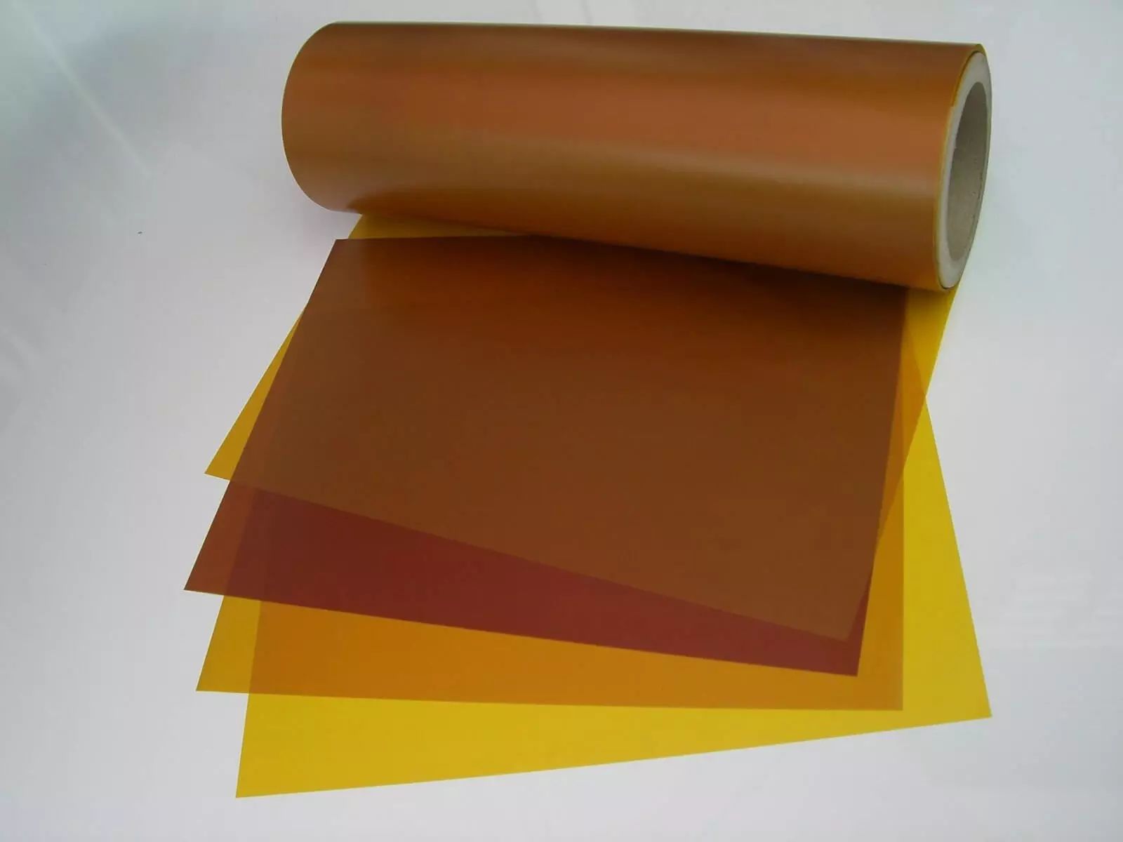
In more applications, we need a flexible plastic film that is more flexible than epoxy. Our most common material is polyimide (PI), which is very soft and strong, and we can't easily tear it or stretch it. Moreover, it has incredible thermal stability, can easily withstand the temperature change of the reflow process during processing, and we can hardly find its telescopic deformation during the fluctuation of temperature.
Polyester (PET) is another commonly used flexible circuit material that has lower heat resistance and temperature deformation than PI film than polyimide (PI) film alone. This material is commonly used in low-cost electronic devices where the printed wiring is wrapped in a soft film. Since PET cannot withstand high temperatures, let alone soldering, it is generally produced by a cold pressing process. I remember that the display part of this clock radio uses this flexible connection circuit, so this radio often does not work properly. The root cause is this poor quality connector. Therefore, we recommend that the soft and hard bonding board still choose PI film, and other materials are also used but not used frequently.
PI film, PET film, thin epoxy resin and glass fiber core are common materials for flexible circuits. In addition, the circuit also needs to use other protective film, usually PI or PET film, sometimes using mask solder mask ink. Like the protective layer protection circuit on the hard board, the protective film can insulate the conductor from the outside to protect it from corrosion and damage. The thickness of PI and PET films ranges from 1â„3 mils to 3 mils, with 1 mil or 2 mil thickness being more common. Glass fiber and epoxy are thicker, typically from 2 mils to 4 mils.
conductor
Printed wires are used in the above-mentioned money-saving electronic products, usually carbon film or silver-based inks, but copper wires are still a popular choice. Depending on the application, we have to choose a different form of copper foil. If it is only to replace the wires and Connectors, thereby reducing manufacturing time and cost, then electrolytic copper foil which is well applied to the compatible circuit board is the best choice. Electrolytic copper foils are also used to increase the current carrying capacity by increasing the weight of copper, thereby obtaining achievable copper skin widths, such as planar inductors.
It is well known that copper has been relatively poor in work hardening and stress fatigue. High-grade rolled toughened copper foil (RA) is a better choice if the flexible circuit in the final application requires repeated folding or repeated displacement. Obviously, the step of rolling toughening is bound to increase the cost, but the rolled toughened copper foil can be bent and folded more times before the fatigue fracture occurs. And it's elastic in the Z-deflection direction, which is what we need, and in applications where it is often bent and rolled, it gives us a longer life. Because the rolling toughening process lengthens the grain structure in the planar direction.
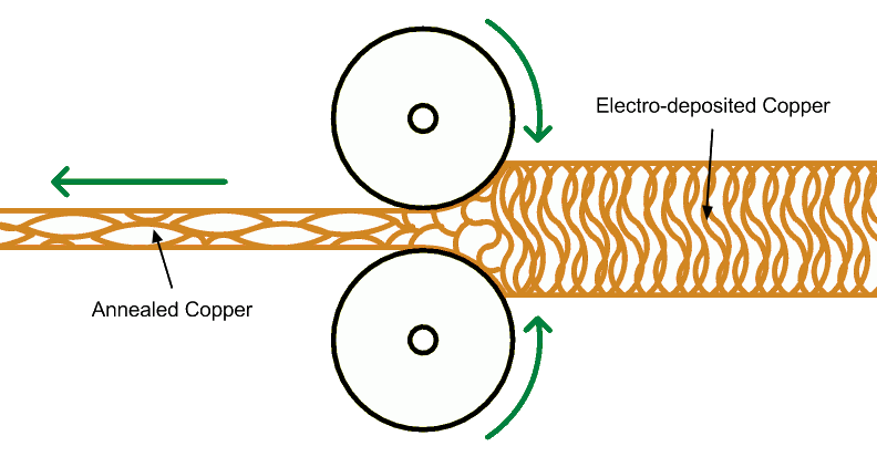
Figure 2: An illustration of the rolling toughening process of an exaggerated version, non-proportional composition. After passing through the high pressure roller, the copper foil can extend its grain structure in the planar direction, making the copper softer and increasing the elasticity of the z-axis.
A typical example is the link between the gantry and the milling cutter head, or the laser head in the blue actuator (as shown below).
 Figure 3: In a Blu-ray machine, the flexible circuit application and the connection between the laser and the main board. Please note that the flexible circuit on the board of the laser head needs to be bent at a right angle. Here, a glue bead is used to enhance the connection of the flexible circuit.
adhesive
Usually, we need adhesives to bond copper foil and PI film (or other film), because unlike the traditional FR-4 rigid plate, the surface of the rolled and toughened copper foil does not have many burrs, so high temperature and high pressure cannot be realized. Good adhesion. Manufacturers, such as DuPont, offer single, double-sided, corrodible copper clad laminate films. It uses an adhesive of 1â„2 mil or 1 mil acrylic or epoxy glue. This adhesive was specially developed for flexible circuit boards.
"Glue-free" laminates are becoming more and more popular due to the introduction of new processing techniques such as direct coating and deposition of copper on PI films. In HDI circuits that require finer pitches and smaller vias, the film can be used in large quantities.
When it is necessary to add protective beads in the soft and hard joints, we will use silicone, hot melt or epoxy. This will increase the mechanical strength of the soft and hard joints, ensuring that no stress fatigue or tearing occurs during repeated use. The best example is shown in Figure 3.
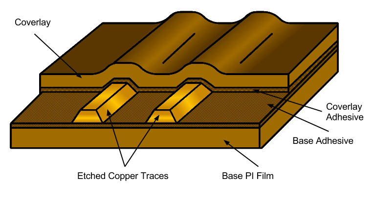
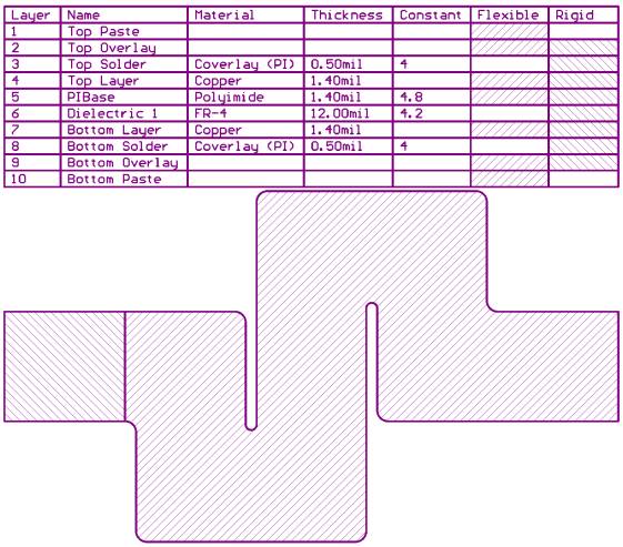
Figure 4: Typical single layer flexible circuit board stack.
to sum up
It is important to understand the materials used in flexible boards or hard and soft boards. We can also give away to manufacturers who can choose materials based on their application, but this creates a hidden danger for the failure of the final product.
Understanding the properties of materials can also help us design, evaluate, and test the mechanical parts of our products. If you are developing a product for automotive applications, heat dissipation, moisture, chemical corrosion, impact, etc., need to be carefully simulated to achieve the highest reliability and minimum allowable bend radius with the right materials. Ironically, it drives us to choose the flexible application of the soft and hard board, which is often exposed to harsh environments. For example, low-cost consumer personal electronic devices are often plagued by vibration, falls, sweat, and the like.
Building a flexible board
At first glance, a typical flexible board or soft and hard board looks very bland. However, making them out requires some extra steps. Making any soft and hard bond board starts with making a single or double sided flexible board. As mentioned last week, manufacturing can start with a pre-compressed soft board, or it can start with a PI film, then laminate the copper plate on the original bare board, or plate it with copper. The lamination process requires a thin layer of adhesive to be applied to the film, and the non-glue process involves seeding the "seed" of copper on the film. The seed is usually seeded by a vapor deposition technique (such as sputtering) to condense the nodules for the subsequent chemical precipitation process. The drilling, plating, and etching processes of the single-sided or double-sided flexible sheets are generally similar to the processing of the double-sided hard boards.
Flexible board manufacturing steps
The following GIF animation shows the manufacturing steps for a typical double-sided flexible circuit board.
 Figure 1: An animated GIF shows the manufacturing process of a flexible circuit board.
1, the application of adhesive or seed "seed"
The use of epoxy or acrylic adhesives, or by sputtering, is the key to creating a thin copper coating.
2, add copper foil
Pressing the RA/ED copper foil layer onto the adhesive (this is the mainstream method) or using electroless plating.
3, drilling
The vias and pads are typically mechanically drilled. Multiple flexible boards can be simultaneously drilled through the work turntable. In the same way as a hard plate, pre-cutting of the flexible board can be performed in combination with drilling, which requires more detailed recording, but the alignment accuracy can be reduced. Laser perforation is typically used to treat ultra-small boreholes, which adds significant cost because each membrane requires separate drilling. Excimer (ultraviolet) or YAG (infrared) is used to process high-precision microvias, and CO2 lasers are used to drill medium-sized holes (4 mils or more). Large vias and plate shears can be handled using stamping, but that is an additional processing step.
4, through hole plating
Once the punching is completed, copper is added to the holes using the same deposition and chemical plating as the hard plates.
5, printing anti-etching ink
A photosensitive resist is applied to the surface of the film and then exposed using the desired pattern to remove the unwanted resist prior to chemical etching of the copper.
6, etching and stripping
After the exposed copper skin is etched away, the resist is chemically stripped.
7, cover film
The top and bottom of the flexible sheet are protected with a cut-form cover film. Sometimes the flexible board needs to be soldered to some components, and the cover film acts as a solder mask. The most common cover film material is polyimide, which is bonded using an adhesive, and a glue-free process can also be used here. In the no-glue process, the photoresist is brushed on the flexible board, which is the same process as the rigid board. In order to reduce the cost, screen printing can be used and then cured by ultraviolet irradiation.
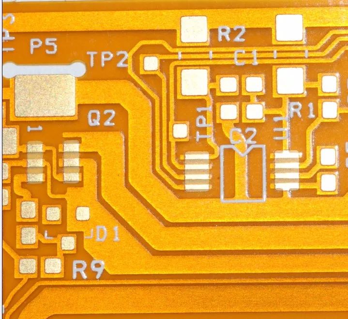
Figure 2: Flexible Circuit with Cover Film - Note that the openings in the overlay are typically smaller than the component pads.
Note that for protective films, it is usually placed only on a portion of the exposed flexible circuit. For soft and hard bonded plates, the protective film will not rest on the rigid plate unless there is a small overlap - usually about half a millimeter. Of course, the protective film may include the entire hard portion, but doing so may be detrimental to the adhesion of the rigid plate and the stability of the z-axis. This optional protective film is called a "bikini protective film" because it covers only the bare parts. In addition, the cover film leaves a slit at the component or connector pad to retain at least two sides of the pad. We will explore this issue in the next blog.
8, the cutting of the flexible board
The final step in making a flexible circuit is shearing. This is often referred to as "cutting." High-yield, low-cost shearing methods use hydraulic presses and steel molds. Although high cost steel molds are required here, this method can cut many flexible boards at the same time. For mold and small batch production, knife molds are generally used. The long blades are shaped according to the contour of the flexible circuit board and then attached to the die base (medium density fiberboard, plywood or thick plastic such as Teflon). The flexible circuit can be cut and formed by pressing the die. For smaller-volume prototype manufacturing, X/Y cutters can be used, some similar to those used for vinyl signage.
Pressing and cutting
If the flexible board is to be pressed into a hard and soft board (the part we are interested in) with the hard board, then I will continue to talk about it. We need to press the flexible board and the hard board together. Like an ordinary flexible board, it requires independent drilling, plating, and etching. The difference is that it is thinner and more elastic due to the lack of fiberglass. As mentioned earlier, plates with less elasticity can be made from PI and fiberglass as needed. Finally, it is also necessary to press it together as a sandwich and a hard board, and make it into a panel.
Laminated laminate
The flexible circuit board is heat pressed together with a rigid circuit board and other flexible boards by an adhesive. Each of the flexible sheets is not adjacent to each other. To maintain flexibility, each flexible board has a maximum of 2 copper layers. The flexible sheets are separated by a hard prepreg, a substrate or a PI core adhesive sheet made of epoxy resin or an acrylate adhesive.
Essentially, each hardboard is individually cut in the portion of the flexible sheet that is filled.
The following is a soft and hard bonding board lamination process in which two two-layer flexible circuits are embedded in three hard boards. The laminated structure is shown in Figures 3 and 4.
 Figure 3: Metal etching, plating, protective film and blank flexible board combined with a glass epoxy hard board.
 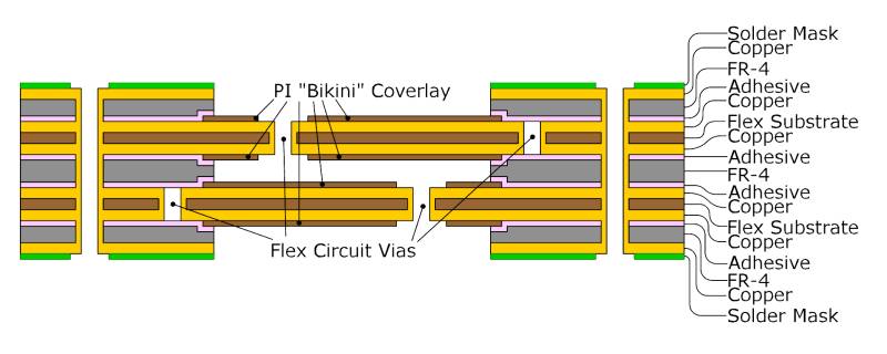 Figure 4: Detailed flow chart including each flexible partially plated laminate and hard partially plated holes.
In the stacked example shown in Figure 4, there are two pre-etched and cut flexible circuits, each of which is double-sided plated. The flexible circuit has been embedded in the final panel, and a rigid circuit board is retained under the flexible circuit for supporting the flexible circuit. This helps keep the flexible circuit flat during the soldering process. There are some potential hazards if the flexible circuit is not supported, such as bending of flexible circuits or large cracks during soldering, especially in reflow ovens. I will mention design-solving techniques in the next blog post.
Solder masks can be coated with a pressure-sensitive adhesive film or with the aforementioned photoresist coating. Finally, after the 6-layer board consisting of the flexible board and the hard board is pressed, the outermost (top and bottom) copper foil layers are joined together. It is usually drilled from the top to the bottom and the coating is completed. It is also possible to use laser drilling blind holes (from the top layer to the flexible board or from the bottom layer to the flexible board), but this will increase the cost.
The final step is to print the top and bottom solder mask, silk screen and anti-corrosion gold plating (eg nickel immersion gold) or solder coating (HASL).
Physical constraint
Multiple flexible board structures
Although in principle the soft and hard bond plates can use a variety of laminate structures, if you fail to carefully consider the production steps and material properties, its cost will be prohibitively expensive. An important consideration in designing a flexible circuit is to understand the pressure within the material when the circuit is bent. After repeated bending, the copper hardens and causes fatigue fracture. One way to alleviate this problem is to use a single layer of flexible circuit structure such that copper is at the center of the bend radius and the film and cover layers absorb the maximum compression and tensile stresses, as shown in FIG. Since polyimide has good elasticity, it is not a problem. Compared to a multi-copper layer structure, a single-layer copper structure can have a longer life cycle in repeated motions.
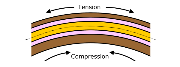 Figure 5: For circuits that require multiple repetitive bends, it is best to use a single layer flexible structure and use RA copper to increase fatigue life.
Similarly, multiple independent flexible circuits are often necessary, but it is best to avoid bending at the overlap because the length of the flexible portion limits the bend radius. Oh! I am a bit too old - design content, I will continue to write more next week...
Glue beads
As I mentioned last week, where the flexible board leaves the hardboard, it needs to be considered to enhance its firmness. Epoxy, acrylic or hot melt adhesives can help to increase the service life. However, dispensing and waiting for it to cure will add extra labor and production cycles.
It is of course possible to use an automatic dispenser, but you must work very carefully with the assembly engineer to ensure that the beads do not fall off after the assembly is complete. In some cases, even time-consuming and expensive, manual gluing is required. Either way, you need to provide the assembler with a clear operating manual.
Reinforcement board and terminal
If not assembled with a hard board, the terminals of the flexible circuit are typically connected to the connector. In this case, the reinforcement section can be added to the terminal section. The material of the reinforcing plate is mostly thicker polyimide or FR-4. Generally, it helps to embed the flexible board onto the hard board.
Jigsaw
In the process of welding, the soft and hard bonding plates are put together. We place and solder the components to the hardboard section. Some products require soldering components on the flexible board. In this case, a hard board is reserved under the flexible board to support the flexible board. The hardboard is not bonded to the flexible board and its contour is milled using a milling cutter of controlled depth. When the welding is completed, the worker can press it down by hand.
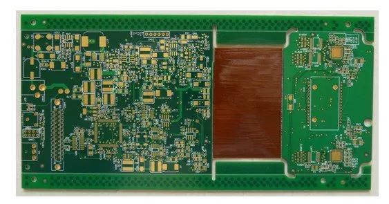 Figure 6: Example of a soft and hard bond plate. Please note that there are front and rear panels, flexible circuits and board cutting. A V-shaped groove has been opened on the hard plate and can be broken after the welding is completed. This saves time during assembly to the chassis.
Manufacturing documents for flexible circuit boards or soft and hard bonded boards
Manufacturing document
Let's talk about manufacturing documents, they are very important. We tell producers what we want by making documents, but they are also important factors that cause misunderstandings or mistakes that lead to costly delays. Fortunately, we can refer to some standards to ensure that we communicate with the manufacturer, especially IPC-2223B.
This can be attributed to the following golden rules:
Make sure your manufacturer has the ability to make soft and hard boards for your design.
Make sure they work with you from the time you build the cascading structure so that the design can meet their production process.
Use IPC-2223 as a design reference and ensure that manufacturers use the same or related IPC standards so that you use the same terminology.
Get them involved in the design process as early as possible.
Output data set
After visiting some local board makers who have the ability to make soft and hard boards, we found that many designers still send gerber files to their board makers. However, the preferred one should be ODB++ v7.0 or higher, because a specific layer type that allows GenFlex ® and similar CAM tools to be clearly identified is added to its work matrix. As shown in Table 1, the subset of data is included.
Table 1: A subset of ODB++ layer types for GenFlex (V7.0 and higher)
(Source: ODB++V7.0 specification)

Layer type | basic type | description |
Cover film | Solder mask | Cover film spacing |
Cover | Solder mask | Cover film spacing |
punch | Shearing board | Mold stamping flexible circuit shape |
Reinforcing plate | Mask layer | The position and shape of the reinforcing plate to be pasted |
Bending area | Mask layer | Identify areas that will bend when in use |
PSA | Mask | Pressure sensitive adhesive shape and location |
area | Description | Definition of area (rigid, flexible or arbitrary) |
Exposure area | Description | The exposed portion of the inner layer and its associated overlay (also available for embedded components) |
Flexible signal | signal | Signal layer of flexible circuit |
Flexible power ground | Plane layer | Power ground plane for flexible circuits |
Flexible mixing | Mixed layer | Mixed layer of flexible circuit |
Coating mask | Mask layer | Area definition that should be covered in a layer during electroplating |
Immersion gold mask | Mask layer | In the process of sinking gold, the area definition that should be covered in one layer |
If you use a file from an earlier version of Gerber or ODB++, we will have a lot of trouble. That is, the manufacturer needs to separate the shear path and die cut pattern of the rigid and flexible circuit portions. In fact, we need to use mechanical layer film to show the avoidance requirements on the rigid board and which parts of the flexible circuit area are exposed; how to use the overlay to reinforce the pads of the components mounted on the flexible circuit.
In addition, particular attention is paid to the pair of drilled holes and the through-hole plating because the drilling from the rigid plate to the reverse side of the flexible board requires re-drilling, which increases cost and yield.
As a designer, the real question is, how do you define these regions, layers, and stacks?
Use a table to define a stacked stack
The most important documents provided to the manufacturer are undoubtedly the cascading stack. In order to make a soft and hard board, it is also necessary to provide different stacks in different fields and to be clearly identified. An easy way to do this is to copy the outline of the board on the mechanical layer and identify the areas where there are different stacked stacks and place the corresponding stacked structure table aside. Figure 1 below is an example.

Figure 1: The stack chart shows the fill pattern of the hard and soft circuit area.
In this example, I used a different stack area matching fill pattern to indicate which stacks are included in the flexible part or the rigid part. It can be seen that the "insulation layer 1" here uses the FR-4 because it is a reinforcing plate.
This creates new problems. We also need a 2D space to define where it is bent or folded, where components and other important objects can pass through the boundary between stiffness and flexibility. I will elaborate on this later.
Passing PCB design intent
We all know that pictures are worth a thousand words. If you can generate a 3D image showing the flexible and rigid areas, this will help the manufacturer to understand our intentions more clearly. Many people now use MCAD software to implement this view. They import the STEP files of the PCB design into the MCAD software. Figure 2 is an example of a reference to this concept.
Figure 2: The bending mechanics model, showing the design intent.
The other benefit is that it helps us to check the mutual interference between the flexible board and the flexible board and between the flexible board and the rigid board to avoid huge mistakes.
Component placement
As you can see from the above figure, the hard and soft bond board means that the components can be placed in the middle layer, not just the top and bottom layers. This is a bit tricky in PCB design software because components must be placed on the top and bottom layers. Therefore, we need the ability to place components in the middle layer.
Fortunately, Altium Designer can place the pads on any layer, so this is possible. In addition, silk screen printing can be printed on flexible circuits. This is not a problem because the cover material is well bonded to the screen printing ink. The key is to choose a strong contrast ink color that passes through the cover material. The sharpness of the silk screen is somewhat affected because it passes through the cover film and the small spacing between them. Again, it is necessary to negotiate with the manufacturer to find a viable and economical approach.
Annotation: If we plan an area on the PCB to connect the flex boards and place components on those areas, then this is a reasonable area for placing embedded components. We need to generate a very clear set of files that show the location and stacking of the cuts. This can be limited by manufacturing methods, such as double drilling or multiple pressing. Therefore, it is important to accurately communicate your intentions and minimize individual openings. It is best to avoid crossing the openings on both sides of the board.
Annotation: Defining FLEX Cuts
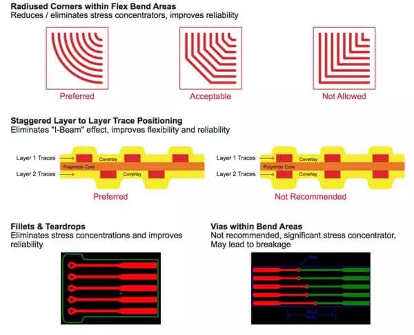
Please note Figure 1, why there are no right angle bends, but what is the minimum radius of each corner? IPC recommends a radius greater than 1.5mm (approximately 60 mils), which greatly reduces the possibility of tearing the flexible circuit at the corners. By the same token, the ends of the grooves and slits in the flexible circuit are to be placed with a diameter of 3 mm (1â„8) or more to prevent tearing. See the example below for details.
Figure 3: The grooves, slits and internal corners should have a circular arc with a minimum radius of 1.5 mm between the lines that prevent tearing or tangency.
In order to produce reliable hard and soft board products, there are many considerations for manufacturers and end users of flexible circuits, including design considerations for copper patterns.
What to do and not to do in flexible circuit routing
Layer stacking, device layout, and clipping are all obvious, and it seems that we have solved them. However, please note that I mentioned in the first blog of this series that there are many material weaknesses in flexible circuits. From the relatively high z-axis expansion coefficient of the adhesive, to the low viscosity PI substrate copper, to copper hardening and fatigue. The following statements and what should be done will largely compensate for the above shortcomings.
Maintain the flexibility of the flexible board
It is obvious to determine the flexibility of the flexible circuit as needed, but we still have to emphasize it again. If the flexible circuit portion is only intended to be folded during assembly and then mounted in a fixed position, for example, in a handheld ultrasound device, then we are selecting the number of layers and the type of copper (RA or ED). There will be a lot of freedom. In the other case, if the flexible circuit part is to be constantly moved, bent or rotated, then the number of layers should be reduced and the glue-free material should be selected.
We can use the IPC-2223B formula (Formula 1 for single-sided, Equation 2 for double-sided, etc.) to determine the minimum allowable bend radius based on the allowable deformation of copper and other material properties.
The formula for this example is for single-sided flexible boards. We choose EB based on actual use. For 16% of applications with few bending applications, 10% for flexible installations and 0.3% for dynamic flexible designs. IPC-2223B, 2008, http://TOC/IPC-2223B.pdf). Dynamic refers to the continuous bending and rotation of the product during use, for example: moving the TFT panel connection in a DVD player.
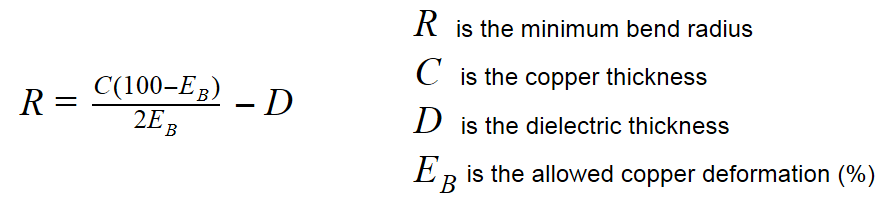
Don't bend at the corner
Usually we recommend keeping the copper trace of the flexible circuit bent in the vertical direction. But sometimes you can't do it, then try to reduce the bending amplitude and frequency, or use the conical bending according to the mechanical design requirements.
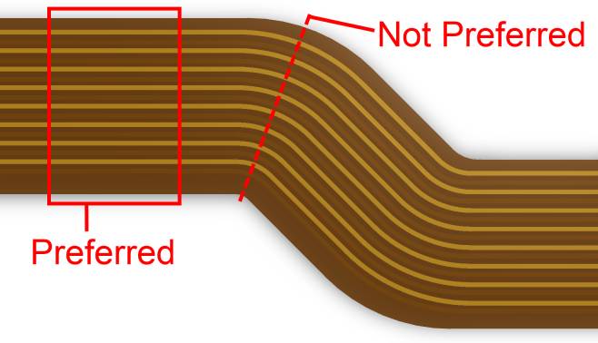
Figure 1: Preferred bending position.
Use curved traces
As shown in Figure 1 above, it is best to avoid the use of abrupt right angles or hard straight 45° angle traces, but instead use the arc angle routing mode. This reduces the stress on the copper during the bending process.
Do not suddenly change the width of the trace
When the traces are linked to the pads, especially the aligned flexible circuit terminals (as shown below), a weak point of stress is formed, which tends to age over time. Unless a stiffener is used or it will not bend during application, the following narrowing of the wiring is recommended (hint: teardrop handling of the pads and vias in the flexible board!)
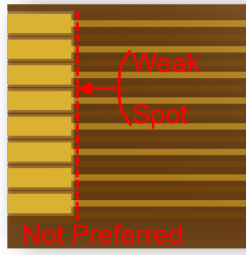 Figure 2: A sudden change in the trace width or a connection to the pad creates a weak point.
Using polygons
Sometimes it is necessary to place a power supply or ground plane on a flexible board. If you don't mind the significant reduction in flexibility and the possibility of wrinkling the copper, you can choose to use solid copper. In general, it is best to use a shadow polygon to apply copper in order to maintain a high degree of flexibility.
Mentioning this, I also thought that the traditional shadow polygon would have extra copper reinforcement in the 0°, 90° and 45° angles. The more optimized mode is the hexagonal mode. This problem can be solved by using the negative layer and the hexagonal pad of the array, and the copy and paste method can be used to create the shadow polygon more quickly.
Figure 3: Uniform balance of stress at three angles using hexagonal copper
Reinforce the pads
Copper on the flexible circuit is more easily detached from the polyimide substrate due to the use of a low tack adhesive (relative to FR-4). Therefore, it is especially important to provide reinforcement to the bare copper. The coated through holes provide proper anchoring for the two flexible layers, so the use of vias is a very good reinforcement. Because of this (providing an extension of the z-axis), many processing plants recommend adding coated vias up to 1.5 mils in the hard and soft bond plates and flexible circuits. The surface mount pads and the uncoated via pads themselves are not reinforced, so additional reinforcement is required to prevent detachment.
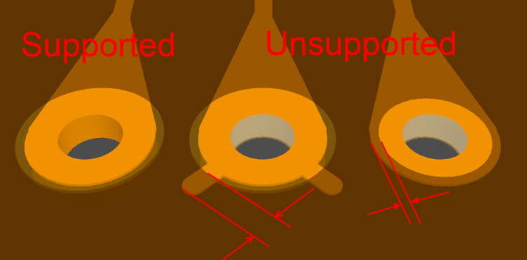
Figure 4: Pad reinforcement for flexible circuits, coating, adding anchoring, reducing the opening of the cover film
Referring to Figure 4, the second option is suitable for a glue-type overlay and the third option is suitable for a glue-free overlay. The protective film using the adhesive will have a phenomenon of "overflow", so the gap between the pad and the opening must be large enough to ensure excellent soldering.
SMT component pads are the most vulnerable, especially where flexible circuits bend under the rigid pins and pads of the component. Figures 5 and 6 show how the overlay is used to reinforce the pads at both ends of the pad. To do this, the pads on the flex board must be larger than the pads on a typical rigid board. Looking at the comparison of Figure 6, the SMD pads of the components are mounted on the flexible board. This significantly reduces the mounting density of the flexible circuit components, but the density of the flexible circuits cannot be too high compared to rigid circuits.
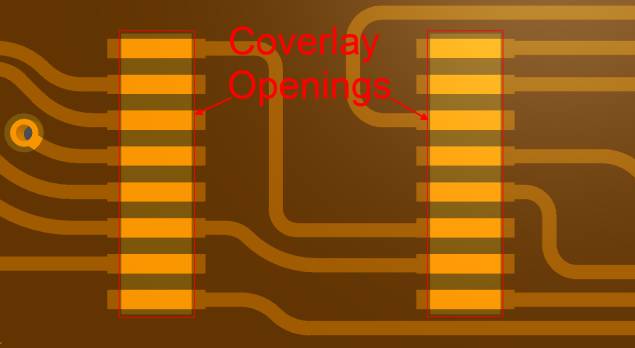 Figure 5: The cover film opening of the SOW package shows its reinforcement at each end of each pad.
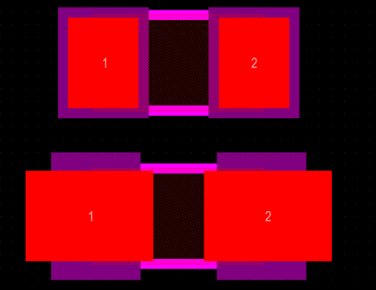 Figure 6: Adjusting the pad size and the opening of the overlay. The above is a typical 0603 package form, the following is a package form modified to use overlay overlay reinforcement.
Maintain double-sided flexibility
For dynamic double-sided flexible circuits, try to avoid placing the wires in the same direction. Instead, you need to stagger them (Figure 7) to evenly distribute the copper traces (Figure 8).
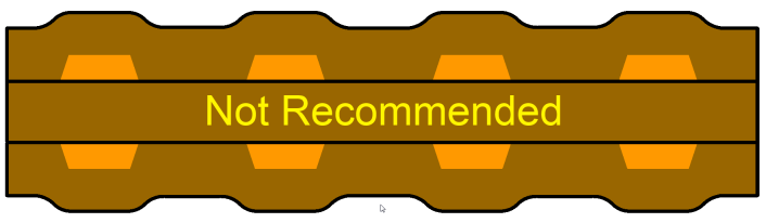
Figure 7: Unrecommended adjacent layer copper traces.
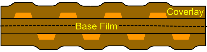
Figure 8: Preferred interleaved adjacent layer copper traces.
Application and examples of printed circuit boards.
As I became more aware of the soft and hard board technology, the more amazing I found out, the more stunning applications. Last week, at Santa Clara, I attended this year's PCB Western Conference. There, I also saw the Altium user base and some old friends! I look forward to discovering some manufacturers and "experts" who are involved in soft and hard productions, and can get some tips, hints and tips from them.
In the past few years, I have heard many flexible circuit manufacturers appear in Sunny California. Moreover, the manufacturers of flexible circuit boards and soft and hard bonded boards have improved in quality, precision and number of layers.
This is great.
So, this week's blog, I want to share with you some of the simple tips and application concepts I have learned. Best of all, there are a lot of board makers who can do these things, and their numbers are increasing every year.
Dynamic and flexible idea
Designing flexible parts in your product is generally based on two principles: first, to build a compact and highly efficient assembly; and second, to integrate the dynamic mechanical structure of the circuit. Of course, the role of the flexible circuit can also be selected according to these two principles. Now let's take a look at a few examples of flexible circuits that inspire your design inspiration.
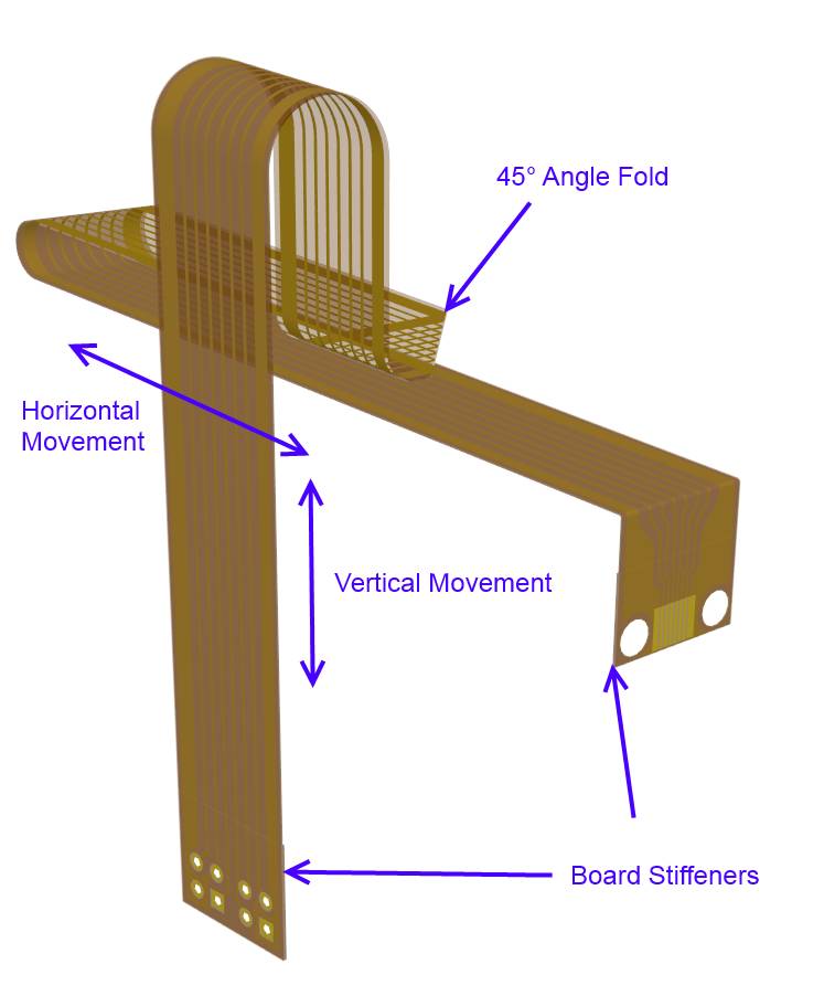
Rack structure
This is a very typical application of dynamic flexible circuits that can be mounted on a 3D printer or on a mechanical head of a CNC machine head. Usually, it will be installed along the X direction and the tool head will move in the z-axis direction. This shows two axial movements, and the frame structure itself moves along the Y-axis.
The total length of the flexible circuit is the length at which the moving head reaches the extreme end, plus the angle of the bend and the length of the bend.
The angled portion is used to connect behind the mechanical head that moves in the Z-axis, which shuttles back and forth along the frame structure with the mechanical head. The terminal of the flexible circuit must be left with sufficient bending length.
For this type of application, it is best to use a single layer of cold rolled annealed copper and the larger the bend radius, the better the design will extend the life of the product.
Sticking the flexible circuit to the stainless steel strip also extends the life of the product.
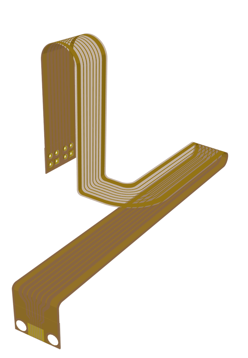 Figure 1: Initial flexible circuit design.
Manufacturing considerations: puzzle
The above example is a good example of a manufacturing and cost issue. If we use a right-angled L-shaped flexible circuit according to the theory, we can make 6 identical flexible circuits on one panel, and we waste nearly 50% of the panel space. If we solder components on top of it, we have to pay extra processing costs and time. The puzzle diagram of this flexible circuit is shown in Figure 2.
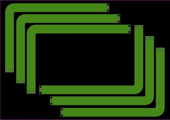 Figure 2: The jigsaw of the flexible circuit of the CNC rack.
Another benefit of using flexibility is that we can design a crease with a very small radius if we use the right material and can guarantee proper installation. This is a good alternative to the previous application, but it should be used in a specific environment.
Figure 3 shows an additional design that uses a 45° crease instead of the 90° corner of the previous design.
In this case, this crease is suitable because this part of the flexible circuit will be fixed to a large rigid mechanical body and therefore will not cause excessive losses.
This solution will significantly reduce costs, and the process of pick and place processing is simplified. However, you may think of this: due to the crease, the component needs to be placed opposite the end of the layer welding assembly.
Figure 4 shows the crease scheme on the same panel, the panel yield doubled!
 Figure 4: The same panel size – the flexible design of the crease scheme doubles the yield per panel!
Planning a stacked structure
The pure flexible electrical layer stack structure is certainly simple compared to the hard and soft bond plates. However, we still need to place anchor points on the panel. Most flexible circuit designs require that a stiffener be placed in the component or termination area of ​​the installation. Figure 5 shows the layer stack structure of a flexible board for the above-described frame structure, the portion of which is a "rigid" stack which is fixedly displayed in 3D in the PCB editor.
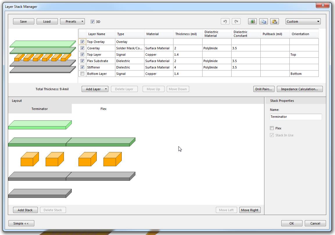
Figure 5: Definition of the layer stack structure of the flexible board used in the rack structure example.
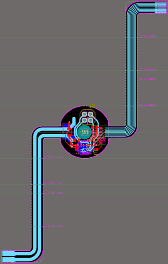
Figure 6: PCB frame with a rotatable flexible design.
Rotating equipment
Looking at Figure 6, in the PCB Editor we used a horizontal working guide that helps to design an accurate plate profile based on the curved circumference of the flexible circuit portion. At the same time, we can also plan and display the crease position of the flexible circuit in the board-level planning mode of the PCB editor, and accurately simulate the bending degree of the flexible circuit board in the 3D mode.
Figures 7 and 8 show a 3D mode view of this design.
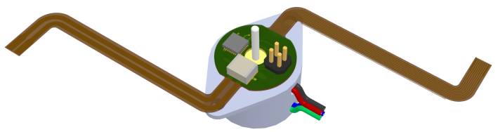
Figure 7: 3D view of the rotary stepper board level. The long "arm" allows the motor and its control board to rotate at an angle of more than 360°.
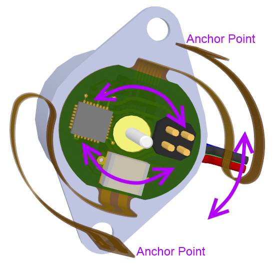
Figure 8: Assembled full folded view, including 3D stepper motor.
In Figure 8, I marked the moving arrows and the fixed ends of the flex circuit to give you an intuitive concept.
This layout design makes it easier to achieve 360° rotation.
This is a hypothetical example, the object is a stepper motor, and this design is very suitable for rotating sensors.
Fixed flexible circuit application
å¹³é¢ç£æ€§å…ƒä»¶ï¼ˆå˜åŽ‹å™¨å’Œç”µæ„Ÿå™¨ï¼‰
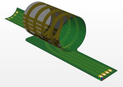
使用柔性æ¿æˆ–者说软硬结åˆæ¿åšå¹³é¢ç£æ€§å…ƒä»¶çš„应用越æ¥è¶Šå¤šã€‚一个月å‰ï¼Œæˆ‘自己维修了我家的43寸液晶电视。当我检查了背光逆å˜å™¨æ¿æ—¶ï¼Œçœ‹åˆ°ä¸€æŽ’æ•´é½çš„å‡åŽ‹DC-DC稳压电路,在稳压电路ä¸ä½¿ç”¨äº†ç”±æŸ”性电路åšç»•ç»„çš„å˜åŽ‹å™¨ã€‚绕组是由旋转的柔性电路构æˆï¼Œå¦‚图9所示。结构的紧凑令人难以置信。
*它的终端连接到贴片ä¿é™©ä¸ä¸Šï¼Œä¿é™©ä¸çƒ§æ–了。现在回想起æ¥ï¼Œæˆ‘当时真应该æ‹å¼ ç…§ç‰‡ï¼Œç»™ä½ ä»¬çž§çž§â€¦â€¦
使用柔性电路åšå¹³é¢ç£æ€§å…ƒå™¨ä»¶æœ‰æ˜Žæ˜¾çš„优势,éžå¸¸è–„çš„èšé…°äºšèƒºè–„膜就å¯ä»¥å®žçŽ°éžå¸¸é«˜çš„安全隔离。而且在很高的的温度下èšé…°äºšèƒºè–„膜还ä¿æŒæ€§èƒ½ç¨³å®šï¼Œè¿™ä½¿å¾—它适用于çƒæªç“·çŒå°å·¥è‰ºã€‚从æŸè€—的角度æ¥çœ‹ï¼Œä½¿ç”¨èš€åˆ»é“œçº¿å›ºç„¶éœ€è¦æ›´å®½çš„èµ°çº¿ï¼Œä½†æ˜¯å› ä¸ºå®ƒå¦‚è‚Œè‚¤çš„è–„åº¦ï¼Œå¯ä»¥éžå¸¸å®¹æ˜“地å‡å°‘涡æµæŸè€—。
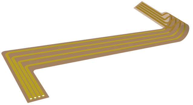
图9:未å·æ›²çš„四绕组电感。
更精致的入å£å’Œå‡ºå£è®¾è®¡ï¼Œèƒ½å¤ŸæŠŠå®ƒä»¬é‡å èµ·æ¥ï¼Œè¿™ä¸ªçš„出å£å¯¹åº”下一个的入å£ã€‚è¿™æ ·çš„è®¾è®¡ä¼šæ¯”åœ¨å¹³é¢ä¸Šè®¾è®¡å¤šä¸ªç‹¬ç«‹çš„ç»•ç»„ï¼Œä¼šæ›´åŠ å®¹æ˜“å¢žåŠ çº¿åœˆçš„åŒæ•°ï¼Œå¦‚图10所示。
 ç”±2层柔性æ¿æž„æˆçš„18层绕组
将这一概念进一æ¥åœ°å»¶å±•ï¼Œæˆ‘们å¯ä»¥åœ¨è½¬æ¢å™¨çš„设计ä¸ä½¿ç”¨ä¸æ›´å¤šçš„柔性层,然åŽæŠŠå®ƒä»¬é‡å èµ·æ¥ã€‚如图11ä¸æ‰€ç¤ºçš„2层柔性电路å˜åŽ‹å™¨è®¾è®¡ï¼ŒE18å¹³é¢é“氧体ç£èŠ¯ç©¿è¿‡PCB上的切å£ã€‚è¿™ç§åšæ³•å¯ä»¥ä»»æ„延伸下去,它的实际é™åˆ¶å–决于最终折å åŽæ¿çš„厚度。如图11,åŒé¢æŸ”性æ¿æœ€ç»ˆæž„æˆäº†18层的å˜åŽ‹å™¨ç»•ç»„。
æ¯ä¸ªåˆ‡å£çš„ä¸å¿ƒï¼Œéƒ½å¯ä»¥æœ‰å•åœˆç”µæ„Ÿç»•ç»„。弯曲轨é“周围的侧边å¯ä»¥æ—‹è½¬åŠåœˆï¼Œç”±äºŽç£è·¯é¢ç§¯çš„侧边实际有效性åªæœ‰ä¸€åŠï¼Œå› æ¤ï¼Œä½ å¯èƒ½æ— 法完全覆盖所有é¢ç§¯ï¼Œä½†é€šè¿‡æ·»åŠ 一个或两个é¢å¤–çš„åŠåœˆåŒæ•°ï¼Œå°±å¯ä»¥å®žçŽ°å…¨è¦†ç›–。

图11:自上å‘下看下柔性电路å˜åŽ‹å™¨ã€‚å•ä¸€å¤§ç”µæµç»•ç»„安装在顶部,å…个å°ç”µæµç»•ç»„安装在底部,å¯ä»¥ä½¿ç”¨Altium Designer总线布线工具实现。
è¿™å¯èƒ½ä¼šé€ æˆæ··ä¹±ï¼Œå› ä¸ºä½ å¿…é¡»è®°å½•æ°å½“çš„é“氧体ç£èŠ¯ç¼ 绕方å‘轨é“。由于整个柔性电路将垂直折å ,我在机械1å±‚æ·»åŠ äº†ç®å¤´ï¼Œä¸Žå„相邻绕组相对,åŒæ—¶æ醒我,哪æ¡éœ€è¦é“ºé“œè·¯å¾„ã€‚ä¸ºè§£é‡Šå¾—æ›´åŠ æ¸…æ¥šï¼Œè¯·å‚åŠ å›¾12。
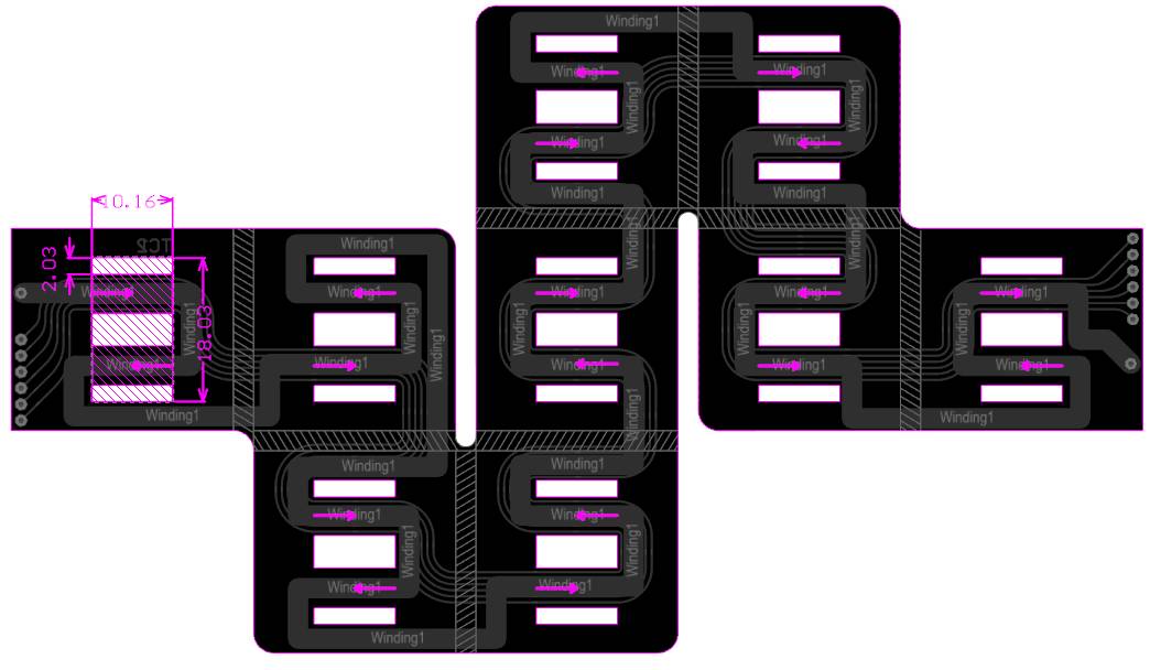
图12:机械1层显示æ¿å±‚轮廓以åŠç»•ç»„æ–¹å‘ç®å¤´æŒ‡å¼•ã€‚
æ ¸å¿ƒçš„æŸ”æ€§éƒ¨ä»¶å®‰è£…å¦‚ä¸‹å›¾æ‰€ç¤ºã€‚è¯·æ³¨æ„,它将与连接到软硬结åˆæ¿ï¼Œé€šå¸¸ç”µè·¯éƒ½æ˜¯åœ¨2层刚性å°åˆ·ç”µè·¯æ¿ä¸Šï¼ŒæŸ”æ€§éƒ¨åˆ†é€šå¸¸æ˜¯æ‰€æœ‰æ ¸å¿ƒç»•ç»„æ‰€éœ€çš„é™„åŠ å±‚ã€‚å½“ç„¶ï¼Œæ˜¯ä½¿ç”¨å¤§é¢ç§¯çš„柔性层,还是在硬性æ¿è®¾è®¡ä¸åŠ 入更多地层,这需è¦æƒè¡¡æˆæœ¬æ¥å†³å®šã€‚
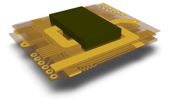 图13 :完全折å çš„å˜åŽ‹å™¨ï¼Œé€šè¿‡åˆ‡å£è¿žæŽ¥3D飞ç£E18é“氧体ç£èŠ¯ã€‚
多层软硬结åˆæ¿
如何ä¿æŒå¤šå±‚柔性æ¿çš„çµæ´»æ€§å’Œè€ç”¨æ€§
许多军事ã€èˆªç©ºèˆªå¤©æˆ–类似的高密度设计,它们需è¦åœ¨ç‹å°çš„空间内实现紧凑布局和å¯é 装é…ã€‚è¿™æ ·å°±å¾ˆéš¾åœ¨ç¡¬æ¿ä¹‹é—´ä½¿ç”¨å¤šå±‚柔性电路。这在高速数å—设计ä¸åŒæ ·éœ€è¦ï¼Œå› 为当总线电路在柔性æ¿ä¸Šèµ°è¿‡æ—¶éœ€è¦æ·»åŠ å±è”½æˆ–者平é¢å±‚。
现在的问题是:为了ä¿æŒè‰¯å¥½çš„çµæ´»æ€§ï¼ŒæŸ”性电路层的数é‡å¿…须尽å¯èƒ½çš„少。通常的结构是一层PI基æ¿ã€é™„ç€åœ¨åŸºæ¿ä¸¤ä¾§çš„铜皮层以åŠPIä¿æŠ¤è†œã€‚
在“普通â€çš„设计ä¸ï¼Œé‡å 的柔性电路的长度是相åŒçš„。如图14展示的情形,一旦装é…完æˆï¼Œé‚£ä¹ˆåœ¨ç¡¬è´¨æ¿é—´çš„æŸ”æ€§éƒ¨åˆ†çš„å¼¯æ›²ä¼šäº§ç”Ÿå¾ˆå¤§çš„å¼ åŠ›ã€‚
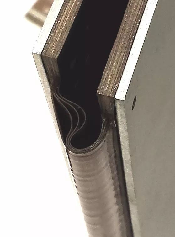
图14:当多个柔性电路é‡å 并有相åŒçš„é•¿åº¦ï¼Œé‚£ä¹ˆåœ¨å¤–éƒ¨çš„æŸ”æ€§ç”µè·¯ä¸Šä¼šäº§ç”Ÿå¼ ä¼¸ï¼Œåœ¨å†…éƒ¨çš„æŸ”æ€§ç”µè·¯ä¸Šä¼šäº§ç”ŸæŒ¤åŽ‹ã€‚è¯·æ³¨æ„,在柔性电路与刚性电路接触部分è¦ä½¿ç”¨èƒ¶ç 。
有ç»éªŒçš„软硬结åˆæ¿åˆ¶é€ 商,会建议使用“装订术â€ã€‚“装订术â€æ˜¯ä¸€ä¸ªå¯è¡Œçš„æ–¹æ³•ï¼Œæ ¹æ®ä½¿ç”¨æŸ”性电路弯曲åŠå¾„æ¥ç¡®å®šå…¶ä»–个柔性电路和基æ¿çš„长度。如图15ä¸æ‰€ç¤ºã€‚
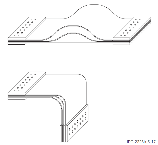
图15:装订术(æ¥æºï¼šIPC-2223B,2008 P26)
ä½ å¯èƒ½ä¼šè¯´è¿™é’Ÿæ–¹æ³•å分费钱,而且对设计æ¥è¯´æ˜¯ä¸ªæŒ‘战。通常更好的替代方法是使用相åŒçš„长度和åŠå¾„的柔性电路,但将ä¸åŒçš„柔性电路层分隔开,彼æ¤ä¸é‡å 。è§ä¸‹å›¾16所示。
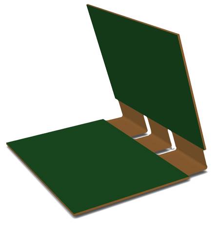 图16:替代的装订术结构。
ä¸æŸå¤±èµ°çº¿å±‚数的超紧密弯曲
如果之å‰æ²¡æœ‰çœ‹è§è¿‡å®ƒï¼Œè¿™ç»å¯¹æ˜¯ä¸€ä¸ªç¥žå¥‡çš„东西ï¼åœ¨PCB西部展会时,我从供应商那儿,æ‹äº†å‡ å¼ è½¯ç¡¬ç»“åˆæ¿å’ŒæŸ”性电路æ¿çš„照片。图17显示了在我大拇指和食指间,是一个å°åž‹çš„电路æ¿ï¼Œå®ƒä½¿ç”¨äº†å‡ 个Så½¢å¶çŠ¶è¿žæŽ¥ï¼Œæ高了å„部分之间的最å°å¼¯æ›²åŠå¾„ã€‚åœ¨è¿™å¼ ç…§ç‰‡ä¸å¯èƒ½çœ‹ä¸å¤ªæ¸…楚清楚,元器件安装在背é¢æœ‰åŠ 强æ¿çš„部分。
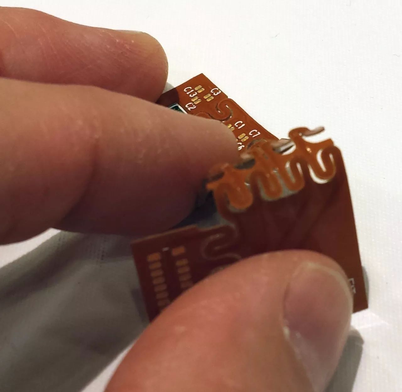
图17:具有多个铜皮层并且ä¿æŒ180°的弯曲。
这一概念当然å¯ä»¥å»¶ä¼¸åˆ°å¤šä¸ªç”¨é€”。如图18所示,这是一个超çµæ´»çš„显示æ¿ã€‚在更宽广的ã€æœ‰åŠ 强æ¿çš„部分上排列ç€ä¸€ä¸ªçš„LED矩阵。整个装é…è¿‡ç¨‹ä¼šæ›´åŠ ä¸¥æ ¼ï¼Œå› ä¸ºå®ƒæ˜¯ç”±å¾ˆå¤šçš„é“œçš®å±‚å’ŒPI膜层压在一起的。åŒæ ·ï¼Œä½¿ç”¨äº†S弯å¯ä»¥ä½¿æ•´ä¸ªè®¾è®¡æ”¾ç½®è¿›å¼§å½¢çš„外壳。我相信,矩阵ä¸çš„æ¯ä¸ªLED都是å•ç‹¬æŽ§åˆ¶çš„,所以在这个设计ä¸æœ‰å¾ˆå¤šç‹¬ç«‹çš„走线。
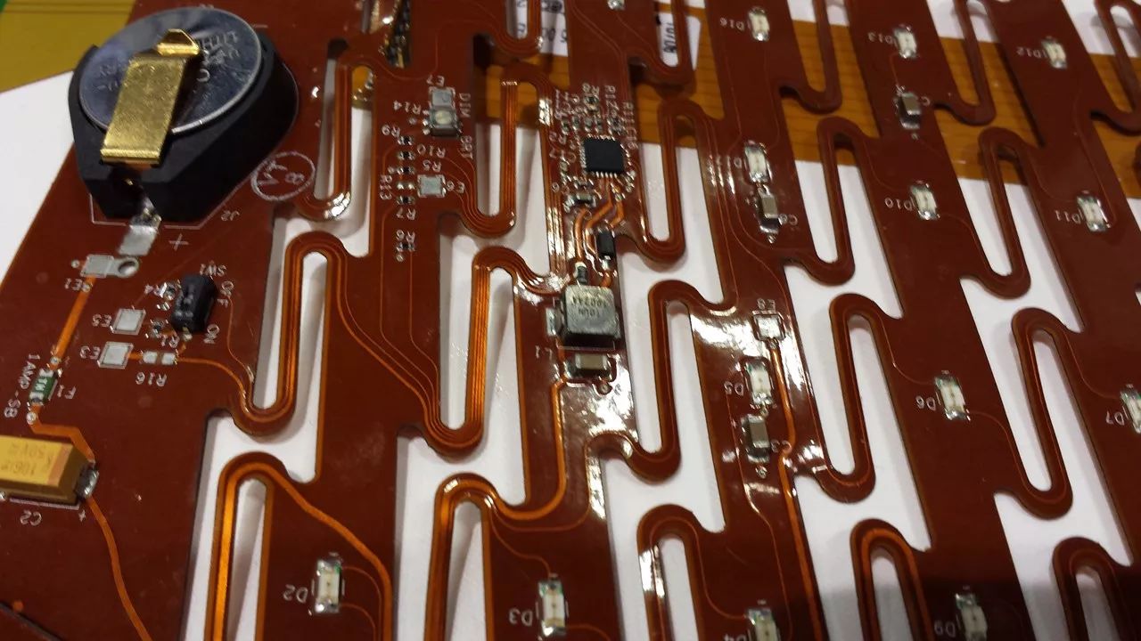
图18:XY S型弯曲柔性阵列。
将这个概念更进一æ¥æ‹“展,图19的应用简直太酷了。这是一个éžå¸¸ç´§å‡‘çš„è®¾è®¡ã€‚æ ¹æ®PCB供应商的介ç»ï¼Œæ¯ä¸ªç‹¬ç«‹çš„柔性电路部分有8å±‚ã€‚è¿™æ ·çš„æŸ”æ€§ç”µè·¯æœ¬èº«æ²¡æœ‰è¶³å¤Ÿçš„çµæ´»æ€§ã€‚但使用多次S弯曲å¯ä»¥ä½¿å®ƒæŠ˜å 到å¯ä»¥è£…进最终的机械外壳,甚至å¯ä»¥åŒ…å«æ•°ç™¾ä¸ªé«˜é€Ÿå†…å˜å’Œæ˜¾ç¤ºè¿žæŽ¥ã€‚注æ„,柔性电路的顶层是实心铜å±è”½ï¼
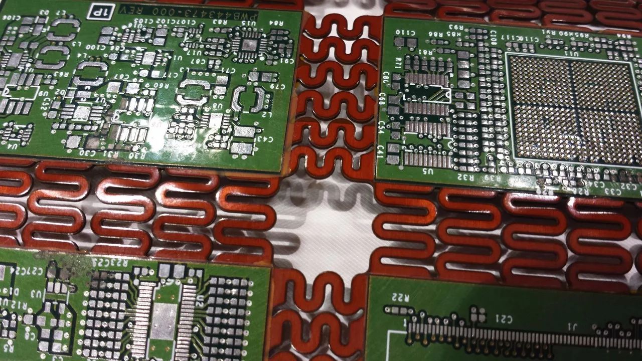
图19: 8层柔性æ¿å±‚å’Œ4个é¢å¤–的硬质æ¿å±‚。注æ„,柔性æ¿çš„顶层是实心铜å±è”½ï¼Œè½¯ç¡¬æ¿ç»“和部分的边缘有粘接剂。
对于æžå…·åˆ›æ„的设计师,总会延伸出更多的应用,如图20所示ï¼
图20:è°è¯´è½¯ç¡¬ç»“åˆæ¿ä¸èƒ½æœ‰æŠ˜ç—•
æ¥æºï¼šå´å·æ–Œåšå®¢ï¼›R Fsister编辑整ç†
转载声明:本文旨在为射频技术圈æ供行业资讯阅读。如有ä¸æ£ç¡®æˆ–ä¾µæƒé—®é¢˜ï¼Œè¯·ç¬¬ä¸€æ—¶é—´è”系我们处ç†ï¼ å°Šé‡çŸ¥è¯†ã€å°Šé‡åŽŸåˆ›ï¼
There are some draft products here, which will not be displayed on the website. These products can be modified later to enrich the content of the website. If you want to know more about our company, you can go to our website to check, there will be what you want, or you can consult us. Nice to meet you and looking forward to our cooperation.
Draft-waiting For Releasing,Draft-waiting For Releasing,Draft-waiting For Releasing
ETOP WIREHARNESS LIMITED , https://www.oemwireharness.com