Application of CPU interface chip GT-48330 in network management switch
1 Introduction
The switch is the most important network connection device in the local area network. Most of the management of the local area network will involve the management of the switch. Switches are classified into managed switches and unmanaged switches. The difference between these two switches is whether they can be managed. Management here refers to operations such as monitoring the port status of the switch, dividing VLANs, and setting trunks through the management port. The switch that can be managed is the network management switch. The network management switch can be managed through serial port, Web (web browser) and network management software.
The internal structure of the network management switch is shown in Figure 1.
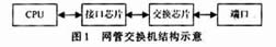
Its working principle: The data packet coming in the port first arrives at the switching chip. The switching chip determines whether it is a management packet. If it is not, it is forwarded through other ports; At the same time, some management packets generated by the CPU are transmitted to the switching chip through the interface chip to control the switching chip, or sent out through the port. In general, the interface chip mainly serves as a bridge between the CPU and the switch chip.
The interface chip and the CPU are usually connected by a PCI bus or a general data / address bus. The interface form with the switching chip mainly depends on the interface of the switching chip. The switching chips of different manufacturers have different interfaces. This article mainly discusses how to use the low-power interface chip GT-48330 to realize the control and management of the switch chip with G.Link interface.
2 Chip Introduction
GT-48330 is the low-power G.Link and CPU interface chip of American Marvell company. He provides a hardware interface between the 8/16 b CPU bus and Marvell's G.Link bus with a G.Link interface switch chip. He supports a variety of embedded CPUs and microprocessors, such as 80C186, 8051, Motorola Coldfire, Inteli960, etc. The CPU can directly manage the switching chip through him. GT-48330, as a low-cost G.Link to CPU interface chip, replaces the PCI interface chip in high-end management systems.
It can be connected with a variety of different CPUs and microcontrollers. The interface data width of its CPU is 8/16 b. It has an on-chip packet buffer. It can cache the entire full-length packet on-chip. The CPU can read through a simple The write operation enters the packet buffer. With an interrupt controller, it can receive interrupts from the switching chip and can generate interrupts to the local CPU or microcontroller. Provide mask and trigger registers. With a core voltage of 3.3 V, the power consumption is low. G.Link clock can be reached
2.1 Interface description
(1) The interface with the switching chip GT-48330 provides 16 transmission data lines GTXD [15: 0], 16 reception data lines GRXD [15: 0] for data transmission with the switching chip; one Send the command line GTXCMD, he is only high in the first clock cycle, indicating that the transmission line is of the command type, the other cycles will be low, indicating that the transmission line is data; a receive command line GRXCMD; a G.Link Clock input line GTXCLK; a reference clock line GTXOCLK for sending data; a reference clock line GRXCLK for receiving data, which needs to be provided by an external clock. A GUNCC line to indicate whether its G.Link port is connected.
(2) Interface with CPU The CPU interface of GT-48330 provides a 16 b data line AD [15: 0] for connecting with the CPU data line; 12 b data line Add [11: 0], used It is connected to the address line of the CPU; a chip selection line CS; a read and write signal line RD and a WR; a working mode selection line Endian, used to set whether the output data high and low bytes are exchanged; one The root address latch signal line ALE; a data return valid line DTACK; an interrupt line INT, used to connect with the CPU interrupt pin; a DTACK mode selection line DTACKMODE, used to determine when DTACK is valid; A configuration line MB is used to determine whether the data and address lines are multiplexed; a mode selection line ASM is used to select asynchronous or synchronous mode; a clock line CLK provides the reference clock for the CPU interface of GT-48330; a RST reset line to reset GT-48330
2.2 Working principle
GT-48330 serves as a bridge between the CPU and the G.Link interface switching chip. The main job is to transfer the data from the switching chip to the CPU. This is a receiving process for GT-48330; it transfers the data sent from the CPU. For the switching chip, this is a sending process for GT-48330.
2.2.1 Reception of GT-48330
The data received by GT-48330 is divided into four types: data packets sent by the switching chip, and new address messages sent by the switching chip (as long as a data packet passes through the switching chip, the source address information in the packet will be recorded by the switching chip And transfer), the interrupt message sent by the switch chip and the message that the CPU wants to read from the switch chip.
(1) Receive data packet process There is a 2 kB buffer (Buffer) in GT-48330 for receiving packets from the switching chip. The packet sending end message (EOP) generated by the switching chip is stored in 0x9E4 0x9EF. When GT-48330 receives the packet and detects EOP, he will send the corresponding interrupt to the CPU. The CPU can obtain the interrupt from the Interrput-cause register Reason, so that the CPU can read packets from the Buffer.
When the Buffer is full, if GT-48330 has not finished processing the previous packet, and a new packet arrives, the G.Link port will be congested. GT-48330 can set the Disable PacketBlocking (DPB) bit to prevent congestion. When set to 0, GT-48330 will send flow control messages to prevent G.Link port congestion; when set to 1, GT-48330 will pass Reject these packets to prevent congestion, at this time all packets will be ignored.
(2) The process of receiving the new address message There is a dedicated new address queue (NA_Q) in GT-48330, which can store 16 entries in total, and the corresponding storage address is 0x800 ~ 0x80F. When a new address arrives, GT-48330 will send an interrupt to the CPU, so that the CPU can go to 0x800 ~ 0x80F to extract the new address message, and at the same time clear the Interrput-cause0 register; if GT-48330 has a new address Address, will put the new address message into 0x800 ~ 0x80F, and issue an interrupt again.
For cases where the new address queue overflows, GT-48330 can handle it by ignoring or sending flow control messages. This can be achieved by setting the Enable_registerbit of GT48330, and the CPU can be obtained by monitoring the NAQOF interrupt. If bit is set to 1, when NA_Q is full, GT-48330 will ignore the incoming new address message; if it is 0, when NA_Q is full, it will send flow control information, notify the switch chip, and postpone sending.
(4) The process that the CPU wants to read messages from the switching chip. The CPU sends a message to the switching chip, indicating that it wants to acquire data (such as some port status information). At this time, the switch chip will send a Block_write message to the CPU. In GT-48330, there is a dedicated 32B Buffer for storing this message. The corresponding storage address is: 0x980 ~ 0x99F. When block_write arrives, GT-48330 will send an interrupt message to the CPU. The CPU obtains the interrupt through the relevant interrupt bit, and then reads the block_write message.
2.2.2 Sending of GT-48330
For GT-48330, he has 2 sending methods: automatic DMA method and CPU transfer method. For the automatic DMA method, no CPU intervention is required, and GT-48330 can automatically complete the transmission. For the CPU transmission method, the CPU needs to interfere with the sending process.
(1) In automatic DMA mode, the CPU first writes the transfer data (TD) register and sets the bits at the same time. GT-48330 sends a Buffer request message to the switching chip according to TD. The TD message contains the destination switching chip number, port number, and CPU number. And the number of packages. The CPU writes data to the 32-bit packet storage space 8LWW Buffer of GT-48330. If GT-48330 receives the message that the switching chip can start to transmit the packet (SOP), he will send the packet to the corresponding switching chip; if received Reject message (Buffer_rejecet) of the switch chip, he will send the corresponding interrupt to the CPU, telling the data to be rejected.
(2) CPU transmission mode The CPU first directly sends a Buffer request message through GNT-A / B Buffer. The CPU waits for the SOP message to be received. This message will be stored in the OGRBuffer by GT-48330 and then transmitted to the CPU. Once the CPU receives the SOP message, it sends the data packet through the GNT-A / B channel of GT-48330, and the CPU also sends the EOP message to the switch chip through GNT-A / B.
3 circuit design
Circuit design description of the G.Link port of GT-48330: the data transmission and reception line GTXD [15: 0] / GRXD [15: 0] is connected to the reception and transmission line of the G.Link port of the switching chip; GTXCMD / GRXCMD transmission It is connected to the receiving and transmitting command lines of the receiving and switching chip; the reference clock of GTXOCLK to send data is connected to the receiving clock of the G.Link port of the switching chip through a matching resistor of 22Ω; the reference clock of GRXCLK to receive data is provided by the clock module ; GTXCLK receives the reference clock of the data, is provided by the clock module; GTXCLK is used as the system clock of the G.Link port of GT-48330, and is also provided by the clock module. The clock frequency of GTXCLK and GRXCLK is 83.33 MHz. The circuit logic diagram is shown in Figure 2.
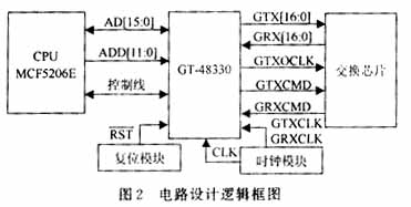
Circuit design description of the CPU interface of GT-48330: The CPU used in this design is Coldfire 5206E from Motorola. Because in the 16 b interface, the MCF5205E data line data is exchanged, that is, D [31:24] means BYTE0; D [23:16] means BYTE1. At the same time, the Endian pin of GT-48330 is pulled down in the design, so that GT-48330 will work in Little Endian mode, and its data is not exchanged, so the data line needs to be exchanged externally, that is, AD of GT-48330 [15:18] Connect with D [23:16] of CPU, connect AD [7: 0] of GT-48330 with D [31:24] of CPU; add-line of GT-48330 address [11: 0] directly connected to the CPU address line A [11: 0]; the chip select signal CS is connected to the CS1 pin of the MCF5206E; after the read / write signals RD and WR of the GT-48330 are connected, they are connected to the R of the MCF5206E / W signal is connected. When R / W is high, the read signal RD of GT-48330 is valid; when R / W is low, the write signal WR of GT-48330 is valid; the address latch signal ALE is connected to the TS signal of MCF5206E, low The level is valid; the interrupt pin INT is connected to the interrupt pin IRQ4 of the MCF5206E to provide an interrupt signal, and the low level is effective; the DTACK of the GT-48330 is connected to the TA of the MCF5206E, the low level is effective, indicating that the data transmission is ended; The signal is directly connected to the output signal of the DSP1832 (or MAX811) of the reset module, which is used to reset the GT-48330 GT-48330, and the low level is effective; the CLK clock is provided by the clock module, and its frequency is 54MHz. GT-48330 will sample some pins during reset to determine the working state of the system. In the configuration, the pull-up is achieved by connecting a 4.7 kΩ resistor to 3.3 V, and the pull-down is achieved by connecting a 4.7 kΩ resistor to ground.
4 software implementation
The software is divided into boot layer (BOOT) and CTRL layer. The MCF5206E starts from BOOT after power-on reset. The functions of the BOOT layer program include power-on initialization, booting or downloading the CTRL layer program and uploading the entire Flash content. The overall software framework is shown in Figure 3.
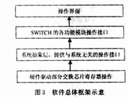
First configure the hardware: including chip selection, DRAM parameters, initialization timer, I / O, etc., and then perform DRAM / CPU ISRAM self-test. If the self-test fails, the corresponding error message is output from the super terminal, and then shut down. If the self-test passes, the integrity of the CTRL layer program is checked. If the CTRL layer program is complete, copy it to the corresponding location of the DRAM and give control to the CTRL layer program; if the CTRL layer program is incomplete, the corresponding information is output through the super terminal And allows to download CTRL layer program or upload the entire Flash content.
The CTRL layer program provides a super terminal interface for setting and testing of various functional modules. The contents of the interface settings are as follows: initial setting and configuration reading, GT48330 register operation, switch chip register operation, Switch function module operation: frame sending and receiving, VLAN setting, trunk operation, port configuration, MIB collection, etc.
After the system is powered on, the power supply module provides power support for the entire system, then the reset module will provide a reset signal to the entire system, and the clock module provides the reference clock to the system. After the MCF5206E and GT48330 modules are reset, the MCF5205E will read the program from the memory module Flash and run it. According to the results of the program, the MCF5205E module will initialize all the switching chips in the system through the GT-48330 module to complete the system. Configuration. In the following process, MCF5206E will use the GT-48330 module to manage the system and receive and send packets. The EDODRAM in the storage module is used to temporarily store the programs and data and packages needed during the operation.
5 Analysis of congestion control
Because the architecture of GT-48330 uses a common FIFO for the received G.Link port, and then through OutMessagerDetecter to determine which channel the data in the FIFO should be sent to, so there may be congestion. If a channel is full, he will no longer accept the data or message that OutMessager Detecter decides to send to him, which will make the data gathered in the FIFO, so that the FIFO is full and congestion occurs.
For the three channels of new address, packet reception, and interrupt reception, an optional mode can be used to prevent congestion, that is, when they cannot receive, they will discard the newly arrived message to prevent it from being congested in the FIFO and causing congestion.
If a lot of data is sent to the packet buffer at the same time, the buffer will be full. At the same time, if it is set to 0 (the packet is not discarded) at this time, the G.Link port will generate flow control messages, causing the G.Link port to Clogged. If the CPU sends an LW_WRITE message to a device at this time, he will always wait for the arrival of Buffer Request Acknowledgement (BFR), and no other data processing will be performed when this message is not received. However, due to the congestion of the G.Link port, the BFR cannot be sent out, so the data in the packet buffer will never be processed by the CPU, which will cause the CPU to deadlock. The solution to the deadlock:
(1) The switch chip can be set to single packet mode (SignalPacket Mode), so that only after a packet is processed, the next packet is sent.
(2) Use Disabled Packet Blocking (Disable PacketBlocking) to prevent new addresses, packet reception, and interrupt messages from being discarded. At the same time, the CPU can also determine potential congestion through certain methods, so that the register is set. For example, you can control the type and number of packets sent to the CPU.
It can be seen from the above that the discard function of the relevant channel can prevent the deadlock problem of the CPU. At the same time, it only affects its own channel; if only the flow control function is used, it may cause the deadlock problem, which will affect the entire G.Link. The mouth has an impact.
1. An open structure of heating elements with half round stainless steel
reflectors for an optimal use of energy.
2. The Gyros will change direction automatice, if there is a force.
3. Removable and detachable parts for easy clean.
4. The particular broiling result is obtained by alternating heating and
cooling down. The meat fibres do not harden, and the gravy is flavoured
by the spices. This cooking mode results in very healthy meat.
5. The Vertical Grill allows broiling meat layers, shashlik, party sausages,
poultry and fish with few attachments.
6. The Skewers and Gyros go in opposite direction so that the food could
be heated more well.
7. Power: 1400W

Vertical Grill
Vertical Electric Grill,Electric Vertical Grill,Vertical Bbq Grills,Indoor Vertical Grill
Housoen Electric Manufacture Co., Ltd. , https://www.housoenappliances.com