introduction
In a certain type of radar signal processing system, the host computer (common PC) is required to monitor the radar system status in real time and collect key variables of the signal processor. This requires a real-time and reliable connection between the processor and the host computer. At the same time, the host computer can also control the signal processing board to complete functions such as processor reset and DSP program dynamic loading. In the experiment, the data transmission distance between the processor and the host computer is not less than 8m. Under this premise, the existing serial and parallel ports on the computer obviously cannot meet the requirements, and the transmission distance of the USB2.0 interface works in high-speed mode is only 3m. Other real-time properties such as Ethernet transmission are difficult to meet the requirements. The construction cost is too high. Based on this, this paper proposes a transmission scheme using LVDS high-speed serial bus technology.
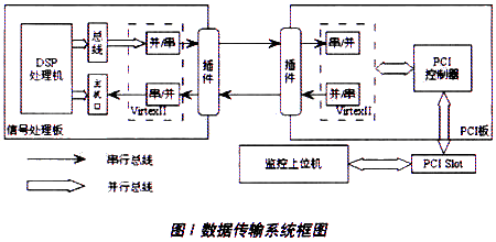
Data transmission system solution
Since the system requires a transmission distance greater than 8m, balanced cables are required. For both ends of the LVDS interface, you can use ASIC and FPGA two ways to achieve. Because the Virtex-II series FPGA produced by Xilinx Company directly supports the LVDS level standard, this system is implemented using XC2V250, which not only saves the dedicated LVDS level conversion chip, saves costs, but also can integrate other control logic in the system into a single In the FPGA chip, the difficulty of PCB design is reduced, and the integration and reliability of the system are improved. In addition, the FPGA of the transceiver interface logic can be used to reconfigure the transmission direction as needed to dynamically change the number of transceiver channels during use, which greatly enhances the reconfigurability of the system.
The block diagram of the entire data transmission system is shown in Figure 1. Since the data transmission is bidirectional, both the signal processing board and the PCI board have a parallel / serial conversion sending module and a serial / parallel conversion receiving module (both are implemented in the FPGA), and the two boards are connected by a balanced cable. In addition, on the signal processing board, the DSP processor sends data to the buffer zone to the FPGA through the external bus, and the FPGA completes data exchange with the DSP storage space through the host port of the DSP. On the PCI board, the FPGA exchanges data with the host through the PCI controller. The working principle of the system can be expressed as follows: The DSP processor outputs the processing result to the FPGA buffer memory through the external bus, completes the parallel / serial conversion of the data in the FPGA, and sends it out through the LVDS serial interface. The data is transmitted to the receiving card of the upper computer through the balanced cable. In the receiving card of the host computer, the data is sent to the PCI interface control circuit after serial / parallel conversion. The process of the host computer outputting data to the DSP processing board is reversed. Because the system requires that the uplink data rate for data transmission is less than the downlink data rate, the number of uplink data transmission channels in the design is 1 and the number of downlink data channels is 4. When the transmission distance is greater than 8m, the actual single-channel data transmission rate reaches 264Mbps.
LVDS Parallel / Serial Conversion Implementation
Because FPGA obtains data through the external bus of the DSP processor, its data form is parallel, so it should be converted into a serial bit stream before sending. The functional block diagram of the module HSTX that implements parallel / serial conversion and serial transmission functions in the FPGA is shown in FIG. 2.
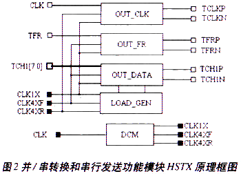
As can be seen from Figure 2, the module has 3 input signals. Respectively, clock input CLK, frame synchronization signal TFR and parallel data TCH1 [7: 0]. Among them, the CLK frequency is 33MHz, and the internal clocks of the serial module CLK1X (33MHz), CLK4XR (33 & TImes; 4 = 132MHz) and CLK4XF (33 & TImes; 4 = 132MHz) are obtained after digital clock manager (DCM) phase-locked frequency multiplication CLK4XR is in antiphase with CLK4XF and in phase with CLK1X. The output is three sets of differential signals, which are serial data TCH1 [P: N], serial clock TCLK [P: N] and serial frame synchronization signal TFR [P: N]. The rising edge of the input clock CLK signal is valid. When the rising edge of the clock, if the frame synchronization signal is high, the input data TCH1 [7: O] is latched, and the transmission is delayed by one clock cycle. The output clock TCLK [P: N] output is 132MHz, and both edges are valid. The output serial data adopts the small terminal mode, the low-order LSB of the data comes first, and the frame synchronization signal TFR [P: N] outputs a bit sequence 11110000 for synchronization at the receiving end.
As shown in Figure 2, the serial transmission module is mainly composed of 4 modules: LOAD_GEN, OUT_DATA, OUT_FR, and OUT_CLK. The LOAD_GEN module is used to generate strobe pulses for loading data during parallel / serial conversion. The OUT_DATA module uses shift registers to implement data parallel / serial conversion. The OUT_FR and OUT_CLK modules are used to generate serial frame synchronization signals and serial clock signals, respectively. These modules are designed using hardware description language VHDL.
LVDS transmission circuit design
Since the transmission rate of the LVDS bus reaches 264Mbps, the requirements for PCB wiring and other aspects are particularly high. This article uses the high-speed circuit simulation analysis tool-Mentor Graphics' HyperLynx to simulate the LVDS transmission circuit, including transmission line impedance design, termination matching, and differential signal wiring. At the same time, the influence of the choice of connectors and transmission cables on data transmission is considered.
The voltage swing of the LVDS signal is only 350mV, which is the current-driven differential signal working mode, and the longest transmission distance can reach more than 10m. In order to ensure that the signal is not affected by the reflected signal when propagating in the transmission line, the LVDS signal requires that the transmission line impedance be controlled and the differential impedance is 100. In the application of this system, the high-speed circuit simulation analysis tool is used to adjust the line width and line spacing by reasonably setting the stack thickness and dielectric parameters, and calculate the single-line and differential impedance results to achieve the purpose of impedance control. The topology of the LVDS signal can be point-to-point unidirectional, point-to-point bidirectional, or bus type (mulTI-drop). No matter what kind of application, it is necessary to perform termination matching at the receiving end. The matching impedance value is equal to the differential impedance, with a typical value of 100. The matching resistor mainly plays the role of absorbing the reflected signal of the load, so it is required to be as close as possible to the receiving end. In this system, the digitally controlled impedance (Digitally Controlled Impedance) in the FPGA chip is used to directly configure the internal termination impedance value of the FPGA to achieve termination matching within the FPGA. This not only facilitates the modification of the terminating impedance value, so that the terminating resistance is well matched, but also the terminating resistance is very close to the receiving end.
The wiring of differential signals is the difficulty of the entire transmission circuit design. Generally speaking, the differential signal wiring according to the impedance design rules can ensure the LVDS signal quality. In actual wiring, LVDS differential signal wiring should follow the following principles:
1. The differential pair should be as short as possible, take a straight line, and reduce the number of vias in the wiring. The spacing of the signal lines within the differential pair must be consistent to avoid too long differential wiring and too many bends.
2. Between differential pairs and differential pairs should ensure more than 10 times the distance between differential pairs to reduce crosstalk between lines. If necessary, place a ground via for isolation between the differential pair.
3. LVDS differential signals cannot be split across planes. Although the two differential signals are the return paths of each other, the cross-division will not cut off the return flow of the signal, but the lack of reference plane causes the impedance discontinuity.
4. Try to avoid using differential signals between layers. In the actual processing of the PCB board, due to the accuracy of the lamination alignment between the laminations is much lower than the etching accuracy of the same layer, and the dielectric loss during the lamination process, the differential signal between the layers cannot guarantee that the spacing between the differential lines is equal to the thickness of the medium Therefore, the differential impedance of the differential pair between layers will change. Therefore, it is recommended to use the difference in the same layer as much as possible.
5. When designing the impedance, try to design it as a tight coupling mode, that is, the differential pair line spacing is less than or equal to the line width.
In addition, high-speed connectors suitable for differential signals should be selected in the design of LVDS transmission circuits. On the one hand, the characteristic parameters of the connector can be matched with the impedance of the LVDS signal, and the signal distortion through the connector is very small; on the other hand, it can provide enough Layout space, design PCB trace width and spacing. For example, AMP's Z-PACK HS3 series connectors are more suitable for high-speed LVDS signal interconnection in terms of electrical performance.
This system uses balanced cables to achieve long-distance transmission. However, due to LVDS's special impedance matching requirements and extremely low timing offset requirements, traditional cables cannot be used for LVDS data transmission. The test confirmed that the performance of the twisted pair cable is the best. CAT3 balanced twisted pair cable works best in short distance (approximately 0.5m) applications. When it is higher than 0.5m and the data rate is greater than 500MHz, CAT5 balanced cable works best.
Conclusion
The high-speed data transmission system implemented in this paper has been successfully applied to data transmission between a radar signal processor and a host computer. The transmission distance is greater than 8m. The data transmission rate of a single channel reaches 264Mbps, and the transmission rate of five data channels totals 1.32GbpS , The transmission process is stable.
FTTx Accessories Clamps & Hooks
Galvanized Steel Pole Clamp,Steel Drop Wire Clamp,Galvanized Steel Hoop Fastening Retractor
Sijee Optical Communication Technology Co.,Ltd , https://www.sijee-optical.com