Design of Computer Network Experiment Platform for C8051F310 and CS8900A
0 Overview
The "Computer Networks" course is a computer and communications professional course offered by university computers and related majors. This course is very practical, and many teaching contents require a high-cost experimental environment to achieve. In addition, the fast update of network equipment and high cost make it difficult for general colleges to bear. Through software technology, the establishment of a software simulation laboratory environment can not only save experimental costs, but also improve the level and quality of experimental teaching.
The development of local area network technology is very rapid, Ethernet (Ethernet) is currently the most widely used local area network technology. Therefore, learning Ethernet technology is very important to master the knowledge of LAN. The purpose of this design is to use the embedded network module to realize the transmission and reception of network data, so that students are familiar with the network data transmission process.
1 Hardware design of the experimental platform
The hardware block diagram of the computer network experiment platform is shown in Figure 1. It is mainly composed of C8051F310, CS8900A, MAX232 and peripheral circuits. 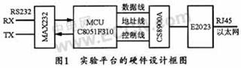
1.1 Microcontroller C8051F310
C8051F310 is a product of American Cygnal company. The device is a fully integrated mixed-signal system-on-chip MCU chip. It is packaged in a 32-pin LQFP and has a small size. The analog peripherals of the C8051F310 include a 10-bit ADC and two analog comparators with rates up to 200 ksps. The power supply voltage of the device is 2.7 ~ 3.6 V, the typical operating current is 5mA @ 25MHz, and the typical shutdown current is 0.1μA. At the same time, C8051F310 also has 1280 bytes of internal data RAM (1 K + 256) and 16 KB of flash memory. Can be programmed in the system, its sector size is 512 bytes. The digital peripherals of the MCU chip include 29 port I / Os, the withstand voltage of all port lines is 5 V, and it has 4 general 16-bit counters / timers. The clock source of the C8051F310 can use either an internal programmable oscillator (24.5 MHz, ± 2% accuracy) or an external oscillator (crystal, RC, C1, or external clock).
1.2 Ethernet control chip CS8900A
CS8900A is a low-power 16-bit Ethernet controller produced by Cirus Logic. It is powerful and its highly integrated design eliminates the need for expensive external components necessary for other Ethernet controllers. The internal structure of CS8900A is shown in Figure 2. 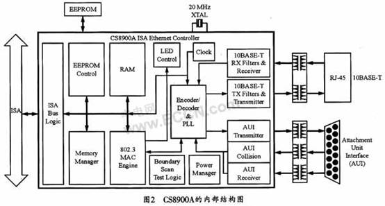
The CS8900A includes on-chip RAM, 10BASE-T transmit and receive filters, and a direct ISA bus interface with 24 mA drive capability. In addition to being highly integrated, the CS8900A also provides other performance and configuration options. Its unique PacketPage structure can automatically adapt to changes in network traffic patterns and existing system resources, so system efficiency is high.
The internal function of CS8900A is mainly 802.3 media access control block (MAC). The 802.3 media access control block can support full-duplex operation, and can fully handle the transmission and reception of Ethernet data frames in accordance with the IEEE802.3 Ethernet standard, including collision detection, frame header generation and detection, and CRC check code Generation and verification, etc. Through the initial configuration of the transmission controller (TXCMD), the MAC can automatically complete the retransmission after the collision of the frame. If the data portion of the frame is less than 64 bytes, it can also generate padding fields to make the data frame reach the minimum length required by 802.3.
The main feature of CS8900A is that it conforms to IEEE802.3 Ethernet standard and has an ISA interface. There is 4K bytes of RAM in the chip, which can be applied to I / O operation mode, memory operation and DMA operation mode. The chip has a 10BASE-T connection port for transmitting and receiving low-pass rates, and supports the AUI interfaces of 10BASE2, 10BASE5, and 10BASE-F. It can also automatically generate a header, automatically perform CRC check, and automatically retransmit after a conflict. The CS8900A has a maximum current consumption of 55 mA (5 V power supply), full-duplex operation, and supports external EEPROM.
After the CS8900A receives the data packet (from the destination address field to the data field, as shown in Figure 3) sent by the host, it can listen to the network line. If the line is busy, wait, otherwise it will immediately send the data frame. 3 shows its 802.3 frame format. 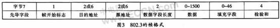
When sending, you should first add the Ethernet frame header (including the leading field and frame start flag), then generate a CRC check code, and finally send this data frame to the Ethernet. When receiving, the data received from the Ethernet frame after decoding, de-frame header and address steps are placed in the buffer. In this way, after the CRC check is passed, according to the initial configuration, the CS8900A informs the host to receive When the data frame is reached, the data is transferred to the storage area of ​​the host in a certain transmission mode.
1.3 Hardware circuit analysis and design
This experimental platform uses C8051F310 as the controller, and the Ethernet control chip CS8900A is also a main working component, used to complete the transmission and reception of network data. The network isolation transformer E2023 is used in conjunction with the chip CS8900A to isolate external lines from the CS8900A, to prevent interference, and to achieve live plug-in function. In addition, CS8900A has two interfaces, one is the RS232 serial interface (level conversion with MAX232 chip) used to connect with the user module, and the other is the RJ45 interface used to connect to the network.
The C8051F310 is connected to the CS8900A through data lines, address lines, and control lines. It can realize the control and read-write operation of the working mode of CS8900A through SBHE, IOW, IOR and so on. When the CS8900A has a hardware reset or a software reset, it will default to an 8-bit operating mode. This design uses 8-bit mode, so that the P1 port of C8051F310 is connected to the lower 8-bit data line of CS8900A. The data transmission between CS8900A and C8051F310 adopts the default I / O mode. Therefore, the read and write pins MEMW and MEMR are set high to close the Memory mode. In this mode, three address lines can be used to access all registers, as long as the pins SA1, SA2 and SA3 are connected to the address line of C8051F310. In fact, except that SA8 and SA9 must be set high to ensure the default offset address (0X300H), all other unused address lines are connected to a low level.
2 Software design of the experimental platform
The software part of this system mainly includes computer program, single chip program and driver of Ethernet chip CS8900A.
2.1 Computer program
The computer program mainly refers to the experimental interface, which is a window for human-computer interaction. Through this interface, students can control and view the sending and receiving process. In this way, when sending data, you can enter the content to be sent, select the protocol used, and control the sending process, and then view and analyze the data of each layer; and when receiving data, you can analyze the use of the received data packet analysis Agreement.
2.2 Driver design of CS8900A
In 8-bit I / O mode, the CS8900A does not support the interrupt mode. Therefore, the C8051F310 uses the query mode to communicate with the CS8900A. Before the CS8900A starts to work, the system must be initialized to determine its working mode. In the process of exchanging data between the host and the network, it is also necessary to continuously read and write the internal registers of the CS8900A. Usually in I / O mode, MCU can read and write all internal registers in CS8900A by operating several main registers of CS8900A. These main working registers are:
â—‡ LINECTL (0112H): Can determine the basic configuration and physical interface of CS8900A. The initial value is 00d3H, the physical interface can be selected as 10BASE-T, and the transmission and reception control bits of the device are enabled;
â—‡ RXCTL (0104H): Control the CS8900A to receive specific datagrams. The initial value is 0d05H, which can receive broadcasts on the network or correct datagrams with the same target address as the local physical address;
â—‡ RXCFG (0102H): It can control the CS8900A to receive a specific datagram and trigger an interrupt. Can be set to 0103H;
â—‡ BLISCT (0116H): Control some operations of the I / O interface of the chip. Set the initial value to 8017H, and the CS8900A interrupt master control bit can be turned on;
â—‡ ISQ (0120H): ISQ is the CS8900A interrupt status register, which can internally map the contents of the receive interrupt status register and the send interrupt status register;
â—‡ PORTO (0000H): When sending and receiving data, MCU transfers data through PORTO;
â—‡ TXCMD (0004H): It is a transmission control register. If data 00C0H is written, the CS8900A will start sending data after all data is written;
â—‡ TXLENG (0006H): Send data length register, when sending data, first write the length of the sending data, and then write the data to the chip through PORTO.
The number in parentheses after the register is the offset of the register address from the base address 0300H. It should be noted that the CS8900A needs to be forced into 16-bit mode before it is initialized.
The host must continuously read and process the interrupt status queue (ISQ) during an interrupt process. When an interrupt is generated, the interrupt pin signal becomes high, and the contents of the five registers are sequentially mapped into the ISQ until 0X000 is read from the ISQ. The software flowchart of its driver is shown in Figure 4. 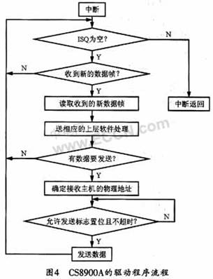
2.3 MCU (C8051F310) main control program
Usually C8051F310 initializes the chip CS8900A first. The initialization part mainly completes the software reset and checks whether the reset completion flag is set; then set the 8 / 16-bit working mode, the default is 8-bit mode; and then set the temporary Ethernet physical address (the real address needs to apply to the authority) After that, when setting the type of received frame, it is generally necessary to be able to receive broadcasts, and then determine the data transmission direction (can be set to full duplex or half duplex), then interrupt permission, enable receive interrupt, and determine the CS8900A interrupt tube Pin number (determined according to hardware line usage), and finally receive and send enable.
When the C8051F310 completes the unpacking of data, it will receive the datagram from the network and analyze the datagram. If it is an IP datagram, it will parse the IP packet and send it to the TCP layer, and then send it to the application layer after parsing the TCP segment. Then unpack the data and output through the serial port. Conversely, if the C8051F310 receives data from the serial port, it will package the data according to the TCP protocol format and send it to the CS8900A after generating the IP packet, and then the CS8900A will output the data to the local area network.
It can be seen that the link layer is completed by CS8900A, while the network layer and the transport layer of TCP / IP are handled by C8051F310, and the application layer is processed by the user as needed.
3 Conclusion
This paper gives the design method of the computer network experiment platform based on C8051F310 single chip and CS8900A Ethernet controller. Through this experimental platform, students can complete the relevant experimental content of protocol analysis. So as to strengthen students' understanding of TCP / IP protocol family.
The connection of the parallel groove clamp for the medium and small section of the aluminum stranded wire or the overhead stranded wire and the steel core aluminum stranded wire strand in the position where the tension is not applied is also used for the jumper connection of the non-linear tower. Parallel Clamp is a parallel connection wire to transmit the electrical load of the contact fittings. Parallel Jaw Clamps are widely used.
The following are the model parameters we product:
| Items | Specification | Sort |
| APG-A | AL 16-70² | Single Bolt |
| APG-B1 | AL 16-35² | Double Bolt |
| APG-B2 | AL 16-70² | Double Bolt |
| APG-B3 | AL 16-150² | Double Bolt |
| APG-B4 | AL 30-300² | Tri-Bolt |
| Item | Specification | Sort |
| CAPG-A1 | CU 6-50² AL 16-70/12² | Single Bolt |
| CAPG-A2 | CU 10-95² AL 25-150² | Single Bolt |
| CAPG-B1 | CU 6-50² AL 16-70² | Double Bolt |
| CAPG-B2 | CU 10-95² AL 25-150² | Double Bolt |
| CAPG-C1 | CU 16-120² AL 16-120² | Double Bolt |
| CAPG-C2 | CU 50-240²AL 50-240² | Double Bolt |
| CAPG-D | CU 35-240²AL 35-300² | Tri-Bolt |
| Item | JBL-16-120 | JBL-50-240 |
| Wire Core Section | 16-120 | 50-240 |
| L | 46 | 46 |
| L1 | 55 | 70 |
| B | 47 | 60 |
| Cat.No. | JBTL-10-95 | JBTL-16-120 | JBTL-16-120 |
| Wire Core Section,mm2 | 10-95 | 16-120 | 50-240 |
| L | 40 | 47 | 45 |
| L1 | 40 | 55 | 60 |
| B | 41 | 48 | 62 |
| Weight,kg | 0.235 | 0.273 | 0.391 |

We warmly welcome friends both domestic and abroad to visit our company, if you have any questions, please contact with us directly.
Parallel Clamp
Parallel Groove Clamp,Parallel Clamp,Parallel Jaw Clamps, Parallel Action Clamp
FUZHOU SINGREE IMP.& EXP.CO.,LTD. , https://www.cninsulators.com