Abstract: This paper presents a design scheme of MP3 player based on portable DAB (Digital Audio Broadcasting) receiver, and introduces the software and hardware design ideas of the system. The system adopts ARM7 single-chip microcomputer as the system controller, uses SD card to store MP3 files, and uses ST company's audio decoding chip STA013 to realize MP3 decoding. The digital voice signal is converted to an analog voice signal by the D/A converter MAX9850 and output by the headphone.
Keywords: digital audio broadcasting; STA013; SD card; audio decoding; MP3
This article refers to the address: http://
INTRODUCTION In recent years, Digital Audio Broadcasting (DAB) has attracted the attention of the international communications and broadcasting industry with its good sound quality, high sensitivity, and high spectrum utilization, and has made rapid progress. The Technical Specification for 30-3000 MHz Terrestrial Digital Audio Broadcasting System, launched by the State Administration of Radio, Film and Television in June 2006, not only enabled DAB to have standard support in China, but also had a significant and positive impact on the popularity of DAB in the country. Considering the popularity of portable MP3 players in today's society and the dependence of consumers on them, the integration of MP3 decoding functions in DAB receivers is necessary for the development of the consumer market. In this paper, based on the original performance of a DAB receiving machine, a feasible scheme for adding MP3 decoding function is proposed.
1 overall system structure
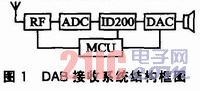
1.1 DAB receiving system structure The DAB receiving system is designed based on a baseband decoding chip named ID200 independently developed by the Key Laboratory of Microelectronics of Chongqing University of Posts and Telecommunications. Its structural block diagram is shown in Figure 1. The U3200 features small area and low power consumption. The MCU uses the AT91SAM7S64 microprocessor from Atmel, which has 64 KB of on-chip high-speed flash memory, 32 programmable multiplexed I/O, SPI and TWI and other rich internal integration resources. The sensitivity of the receiving system can reach -97 dBm or more in the 3 and L bands. MPEG L2 audio source decoding, support 48 kHz and 24 kHz sampling frequency, automatic recognition of channel mode, support single channel, dual channel, stereo.
1.2 Main device selection Taking into account the DAB receiver's baseband decoding chip has not yet added MP3 decoding function, as well as production cost, microcontroller speed, chip maturity and other factors, the ST013 decoder chip of ST company is adopted. The chip has the following features: support MPEG1, MPEG2 and MPEG2.5 format decoding; support stereo, dual channel, mono decoding; support 8 ~ 320 kbps compression rate; serial bit stream input and PCM output interface, support I2C Bus; low power consumption, 85 mW at 2.4 V; 10 MHz, 14.31818 MHz, 14.7456 MHz external input clock, or embedded industry standard XTAL crystal to meet different frequency requirements.
Since the STA013 does not have the function of a DAC and a headphone amplifier, a DAC chip is required, and Maxim's MAX9850 chip is used here. The chip is a low-power, high-performance stereo audio DAC that integrates a direct-drive headphone amplifier that allows the amplifier output to directly drive the headphones, eliminating the need for large DC-blocking capacitors, saving cost and wiring space, while also providing an I2C bus and PCM output interface.
Considering the development of the portable whole machine and the popularity of the memory, this solution uses the MicroSD card as the audio data storage unit. MicroSD card is ultra-small, but has many advantages such as high transmission speed, strong mobility, safety and reliability. It can be applied to all kinds of digital products without wasting space for internal design. At the same time, it uses FAT16/32 file system and provides SPI interface for consumer file download and management.
2 Scheme principle and design ideas
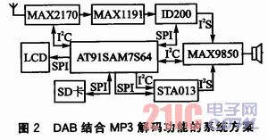
2.1 Scheme Principle The scheme of integrating the MP3 decoding function in the DAB receiver is shown in Figure 2. Here mainly introduces the part related to MP3 decoding. The AT91SAM7S64 microprocessor utilizes the chip select line of the SPI interface to communicate with up to four slave devices. In the system, four SPI chip selection lines of the MCU are selected as ID200, MicroSD card, STA013 and liquid crystal display module. The RF chip and ADC are selected from Maxim's MAX2170 and MAXll91, respectively. The MCU reads the audio data in the SD card into the buffer in the MCU through the SPI bus, and then sends the data to the STA013 through the SPI bus for audio decoding, and the decoded audio data stream can be sent through the PCM output interface. The MAX9850, after D/A conversion and headphone amplifier, is ultimately output by the headphones.
STA013 mainly relies on the I2C bus to transmit control information, and the serial data line receives audio data. The serial data line consisting of three pins SDI, SCKR, and DATA_REQ can be regarded as an SPI bus with only SIMO (slave input host output) and no SOMI (slave output host input). When DATA_REQ is set high, the data in the MCU buffer is input to STA013 through the SDI pin as fast as possible, and the serial clock is supplied to the decoder chip using SCKR. When STA013's buffer overflows quickly, DATA_REQ is set low and data stops transmitting. The MCU's I2C bus is connected to the STA013's I2C interface, which uses it to transmit commands, initialize the decoder chip, and control the decoding process.
2.2 Design Ideas The connections of the modules in the MP3 decoding system are shown in Figure 3. The SD memory card system defines two communication protocols, SD and SPI, and one of the modes can be selected for application. Since the AT91SAM7S64 used in this solution does not provide the hardware SD bus interface, it provides the SPI bus interface. In order to avoid the software to simulate the I/O port as the SD bus interface, the SPI bus mode is used here for the Micro SD card and MCU. Command and data communication between. When the SD card is powered on, it is always in SD mode. If the system wants to use SPI mode for communication, it can enter the SPI mode by setting the master chip select (SD_CSN) signal low during the SD card to send the reset command CMD0. By powering down and then powering up, the SD card system can be returned to SD mode. MicroSD cards are stored in clusters. There are 32 sectors in a cluster, and each sector can store 512 bytes of data. Since the SD card, STA013, and liquid crystal communicate with the MCU through the SPI bus, it is necessary to handle the timing of the bus communication. The SPI bus that is turned on during the initialization of the SD card needs to be closed after acquiring the card information, and then the SPI interface of the LCD is turned on; when the MP3 program is played, the SPI of the LCD needs to be turned off, and the SPI bus of the STA013 is turned on.
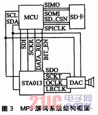
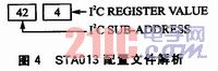
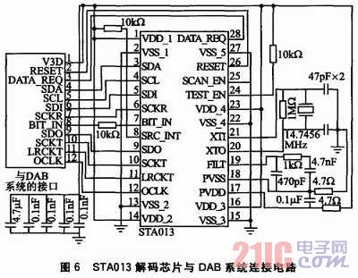
The STA013 decoder chip has three important interfaces, namely the serial input interface, the I2C interface, and the PCM output interface. The SDI and SCKR of the serial input interface are respectively connected to SIMO and SPICLK in the SPI bus of the MCU, and the DATA_REQ provides an interrupt signal to the MCU. The PCM output interface is connected to the I2S interface of the DAC, and the MCU controls the MCU and DAC through the I2C bus interface. When initializing the STA013 chip, the configuration file provided by ST must be written through the I2C bus interface. In this file, the odd-numbered data is the I2C register address, and the even-numbered data is the default value of the corresponding I2C register. The STA013 configuration file is parsed as shown in Figure 4. The I2C addresses of STA013 and DAC are 100011 and 0010011, respectively, so there is no device conflict when multiplexing the I2C bus interface of the MCU.
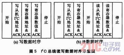
The I2C bus interface read and write data timing is shown in Figure 5.
The circuit diagram was drawn using Mentor's PADS software. The connection circuit based on the STA013 decoding chip and each part of the DAB system is shown in FIG. 6.
MP3 decoding workflow:
1 initialization of the decoding chip. Initializing STA013 includes the following steps: hardware reset STA013; SPI initialization; writing the configuration file provided by ST company to the decoding chip through I2C interface; working mode of decoded PCM data, PLL, decoder working mode and input bit stream clock polarity Wait for configuration.
2 transmission of audio data. Since STA013 has a strong decoding function, when STA013 needs data (DATA_REQ is high), it must be transmitted to it through the SDI interface as fast as possible (but below 20 Mbps). This can be done by setting the SPICLK of the SPI bus, where the SPI clock is set to 4 MHz. Data is sent from the MCU to the buffer of the decoder chip in units of sectors. Note that when transmitting data with SPI, the BIT_EN port must be set high for efficient transfer. STA013 automatically determines the data input and output transfer rate, and when its buffer memory is saturated, it will terminate the data request. For variable MP3 data of the bit stream, STA013 can also handle it automatically. In addition, it can properly adjust the DAC clock based on the automatically detected sampling frequency of the MP3.
3 decoding of audio data. By obtaining the MP3 file frame header to obtain some decoding parameters, it automatically adapts to the decoding of different MP3 audio streams. For example, the output clock frequency of the audio, etc., can be automatically adjusted by the sampling frequency in the decoding parameters.
4 The output of the audio stream after decoding. STA013's SDO (PCM serial data output), SCKT (PCM serial clock output), OCLK (sampling clock) and LRCLK (left and right channel clock output) pins can be paired with the SDIN (serial data input) of the MAX9850. , BCLK (digital audio bit clock input), MCLK (main clock input) and LRCLK (left and right channel clock input) are connected. After the decoded audio stream is converted into an analog audio signal by the DAC, the full PCM audio can be output from the earphone through the headphone amplifier.
Conclusion The design MP3 decoding scheme is based on a DAB receiver. Since the baseband decoder chip ID200 used in this DAB receiver has extremely low power consumption (26 mW/128 kbps), the MP3 decoding function must first be considered from the power consumption and cost of the whole machine. The STA013 decoder chip not only meets the requirements of low power consumption, but also has a price advantage and high technical maturity, so it has become the first choice for solution design. However, its volume is relatively large, and should be optimized in PCB layout to meet portable requirements. With the rapid popularization of digital broadcasting in China and the maturity of DAB technology, the integration of MP3 decoding function into the DAB baseband decoding chip plays a vital role in improving the portability and ease of development of the whole machine. An important direction to optimize the design in the future.
Socket Cover,Metal Socket Cover,Aluminum Power Outlet Cover,Aluminum Power Sockets Cover
Dongguan baiyou electronic co.,ltd , http://www.dgbaiyou.com