The 7 Series FPGAs are Xilinx's new 28nm process-based FPGAs, which include three families: ArTIx, Kintex, and Virtex. Because the project needs to use kintex7 as the platform for design, it needs to study its internal structure, starting with CLB (Configurable Logic Block):
CLB constitutes the main logic unit of Kintex7, which contains 2 slices, and Slice is divided into 2 kinds: SLICEL and SLICEM, SLICEL is a common Slice logic unit, and SLICEM can be extended to distributed RAM or shift based on basic logic functions. Bit register. Of all the Slice resources, 2/3 are SLICEL, so a CLB can have 2 SLICELs or 1 SLICEL and 1 SLICEM.
Figure 1 shows the internal structure of SLICEM, which consists of four 6-input LUTs (red circles), a carry chain (yellow circle), a multiplexer (blue circle), and eight registers (green circles).
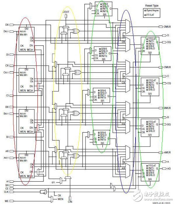
6-input LUT: Here the LUT follows the 6-input LUT structure of the Xilinx 6 series FPGA. The 6-input LUT consists of two 5-input LUTs, with two outputs corresponding to O?6 and O5. In the design, if there are two 5-input LUTs to be used after synthesis, if the integrated option -lc (LUT Combining) is set to Area in ISE, the synthesizer XST will merge the two 5-input LUTs into one. -input is implemented in the LUT, but this option is equivalent to changing the area by speed, and the logical delay will increase.
Register: Here Xilinx is different from Altera devices. One LUT corresponds to two registers, and Altera devices have one-to-one correspondence. As you can see from the figure, the register in column 2 has more FF/LAT option than column 1, which means that the register in column 1 can only be used as Flip-Flop, and the register in column 2 can be used as Flip-Flop. Can also be used as a Latch. There are also four options: INIT0, INIT1, SRLO and SRHI, where INIT0 and INIT1 are paired, indicating that global reset/set by GSR, this reset/set network is asynchronous; and SRLO and SRHI are paired, indicating active high. Signal SR driven reset / set, this signal can be configured to be asynchronous or synchronous, but these 8 registers share an SR signal, so the mode must be the same, according to this feature, it is recommended to write the code, reset / set mode select synchronization Active high.
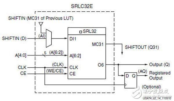
The following is a highlight of SLICEM, which can be extended into a shift register. As shown in Figure 2, each LUT in the slice can be configured as a 32-bit Shift Register, so a slice can be expanded to a maximum of 128-bit. Shift Register. Its operation mode is 1 clock cycle shift, input through D input, and the last 1 bit is output through MC31, and can be selected by A[6:2] as a 5-bit address to select one of 32 bits of O6 output. Output.
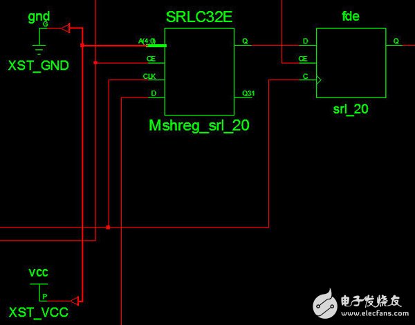
When writing code, you can write the form of the shift register as specified, as shown in the following code:
Always@(posedge clk)
If(clk_en)
Srl<={srl[31:0], din};
Assign dout0=srl[20];
The structure synthesized by the above code is shown in Figure 3. The synthesizer uses only one LUT and one FF to implement a 21-bit shift register, requiring only one slice.
If you click on the code to synthesize the structure, as shown in Figure 4, the synthesizer uses 21 FFs to implement the 21-bit shift register, which requires 21 slices.
Always@(posedge clk)
If(rst)
Srl<=32'd0;
Else
If(clk_en)
Srl<={srl[31:0], din};
Assign dout0=srl[20];
Why does the synthesizer produce a different structure? Analyze the difference between the code, the second code has a synchronous reset function compared to the second code. According to the structure of SLICEM, the LUT has no synchronous reset control input, so the synthesizer can't integrate the code into the idea. The structure you want, so you need to write the code according to the corresponding structure.
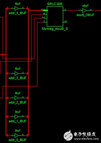
Looking at Figure 3, we can find that an FF is connected to the output of the SRLC32E as a synchronous output. After checking the manual, the shift register can be configured into two output modes: static address mode and dynamic address mode. The difference between the modes is that the static address mode is synchronous output, the structure in Figure 3 is the static address mode; and the dynamic address mode is the asynchronous output, that is, there is no subsequent FF output directly from the Q terminal of the SRLC32E, and the following code indicates the dynamic address mode. Where addr is a variable.
Always@(posedge clk)
If(rst)
Srl<=32'd0;
Else
If(clk_en)
Srl<={srl[31:0], din};
Assign dout0=srl[addr];
Combining the above code can get the structure shown in Figure 5, and determine that the output is an asynchronous output, so pay attention to the changes here in the design.
3.5 Mm Audio Jack Panel Mount,3.5 Mm Panel Mount Jack,Audio 3.5 Mm Port,3.5 Mm Aux Port
Dongguan Swan Electronic Technology Co., Ltd , https://www.swanconnector.com