ChipScope Pro provides debug cores for many different functions, usually divided into three categories: logic debug cores, bit error rate test cores, and integrated bus analysis cores. According to the debugging requirements of the system, the user applies different debugging kernels to quickly and easily find the problems in the design. A common IP core is shown in Figure 9-3.
(1) Logic debug kernel.
ICON (Integrated Controller Core).
ILA (Integrated Logic Analysis Core).
VIO (virtual I/O core).
ATC2 (Agilent Tracking Core).
(2) IBERT (bit error rate test core).
IBERT (bit error rate test core) for the Virtex-4 FX platform.
IBERT (bit error rate test core) for the Virtex-5 LXT/SXT/FXT platform.
IBERT (bit error rate test core) for the Virtex-6 LXT/SXT platform.
IBERT (bit error rate test core) for the Spratn-6 LXT platform.
(3) IBA (Integrated Bus Analyzer).
IBA/OPB (Integrated Bus/Processor Peripheral Bus Core).
IBA/PLB (integrated bus/processor local bus core).
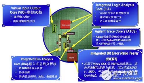
Figure 9-3 IP Core of Common ChipScope
I. ICON coreThe ICON core has the ability to communicate with the JTAG boundary scan port, so the ICON core is an essential core for ChipScope Pro applications. An ICON core can connect up to 15 ILA, IBA/OPB, IBA/PLB, VIO, or ATC2 cores simultaneously. In the Virtex-4/5/6 and Spartan-6 chips, the USER1, USER2, USER3 or USER4 scan chain can be used with the BSCAN_VIRTEX primitive, and since the BSCAN_VIRTEX primitive implements a separate scan chain, there is no need to export Unused user scan chain. In the remaining types of chips, only the USER1 or USER2 scan chain can be used.
Second, the ILA coreThe ILA core provides triggering and tracking functions to capture data based on user-set trigger conditions, then upload data to the PC via the boundary scan port under ICON control, and finally display the signal waveform in the analyzer (Alalyzer). Since the ILA core and the monitored logic are synchronous, all clock constraints in the design are applied to the ILA core. The ILA includes the following three main components:
Input and output trigger logic: Input trigger logic is used to detect various trigger conditions; output trigger logic is used to trigger external test equipment and other logic.
Data Capture Logic: Data capture logic is used to capture data and store the captured data in the chip's BRAM.
Control and Status Logic: Control and status logic is used to manage various operations of the ILA.
Third, the VIO coreThe VIO (Virtual I/O) core is a virtual console for real-time monitoring and control of the internal logic signals of the FPGA. It can observe the output signals of any module in the FPGA design, and can also add virtual inputs to these modules, similar to DIP switches and buttons. Etc., and does not occupy BRAM resources. The VIO core is module-oriented and supports the following four types of signals:
Asynchronous input signal: Asynchronous input signal, clocked by the JTAG clock signal (TCK), periodically read into the PC, and the result is displayed in the user interface of the ChipScope Pro analyzer.
Synchronous input signal: Synchronous input signal, clocked by the clock in the design, periodically read into the PC, and the result is displayed in the user interface of the ChipScope Pro analyzer.
Asynchronous output signal: Asynchronous output signal, defined by the user in the ChipScope Pro analyzer, sent to the surrounding logic, the logic "1/0" of the output signal is defined by the user.
Synchronous output signal: Synchronous output signal, defined by the user, synchronized with the system clock, the logic "1/0" of the output signal is defined by the user.
Fourth, ATC2 coreThe ATC2 core was developed in collaboration with Xilinx and Aglient and is used in conjunction with Agilent's latest generation of logic analyzers. The block diagram of the ATC2 core is shown in Figure 9-4. It can be viewed as a configurable multiplexer with inputs for some signal groups and up to 64 groups.
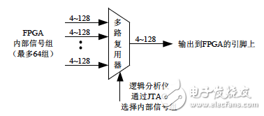
Figure 9-4 ATC2 structure diagram
An FPGA dynamic detector application running on the Agilent logic analyzer allows it to observe the signals output from the FPGA.
ATC2 enables the joint debugging and capture of data between the FPGA and the Aglient logic analyzer, allowing the Aglient logic analyzer to access any node inside the FPGA, providing deeper capture depth, more complex trigger settings, and support for network remote debugging. Reduces the use of BRAM compared to using ChipScope Pro alone.
The ATC2 is connected to an Anlient logic analyzer that provides 2M capture depth per signal, 60 times that of ILA. In addition, up to 64 observation signal groups can be added inside the FPGA, and the logic analyzer can be connected up to 128. This is very helpful in finding design flaws.
Five, IBERT coreThe IBERT core is used to measure bit error rates on multiple channels of high speed serial transceivers and to adjust high speed serial transceiver parameters in real time. The BERT core consists of three parts.
BERT Logic: The BERT logic instantiates the RockeTIO transceiver block, which includes the pattern generator and detector. There are several modes to choose from, including simple clock mode, full pseudo-random binary sequence (PRBS) mode, and frame count mode.
Dynamic Reconfiguration Port (DRP): Each Rocket I/O transceiver has a dynamic reconfiguration port, so the transceiver properties can be dynamically changed.
Control and Status Logic: Manage the IBERT core.
Sixth, IBA/OPB coreThe soft-core processor MicroBlaze can be embedded in Xilinx's FPGA. In some high-end devices, there is IBM's hard processor core PowerPC. The IBA/OPB core is dedicated to the on-chip peripheral bus (OPB). The IBA/OPB core consists of four main parts:
Protocol conflict monitoring: Monitor and report OPB bus collision events, up to 32.
Input and output trigger logic.
The trigger input logic monitors the OPB bus and other user defined events.
The trigger output logic triggers external test equipment and other logic.
Data capture logic: used to capture data and store the captured data in BRAM.
Control and Status Logic: Manages IBA/OPB core operations.
Seven, IBA / PLB coreThe IBA/PLB core is dedicated to connecting the on-chip peripheral bus (PLB). The IBA/PLB core consists of three main parts:
Input and output trigger logic.
The trigger input logic monitors the OPB bus and other user defined events.
The trigger output logic triggers external test equipment and other logic.
Data capture logic: used to capture data and store the captured data in BRAM.
Control and Status Logic: Manages IBA/PLB core operations.
Note: The IBA/PLB core is only used for PLB versions prior to PLB v46. The XPS tool provides an IBA core (chipscope_plbv46_iba) for debugging in PLB v46.
Shenzhen Ousida Technology Co., Ltd , https://www.osdvape.com