In order to adapt to more and more complex DSP operations, Spartan-6 continues to expand its functions on the Spartan 3A DSP module DSP48A, and introduces the more powerful DSP48A1 SLICE.
Figure 2-31 shows the functional block diagram of DSP48A1. The arithmetic part contains 18-bit pre-adder, two 48-bit data input multiplexers (outputs X and Z), 18 & TImes; 18-bit twos complement multiplier, followed by A 48-bit wide symbol expandable post-adder/subtracter/accumulator.
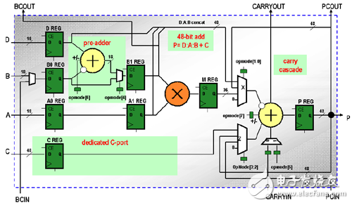
Figure 2-31 Functional Block Diagram of DSP48A1
The data and control inputs of the DSP48A1 are connected to the arithmetic and logic sections. There are two stages of pipeline registers on the A and B input channels. Other data and control input channels also have a level one pipeline register. The maximum operating rate is 250MHz (in the lowest speed class device) when using the pipeline registers.
The structure adapts to many functions in the DSP application, its programmable pipeline structure, 48-bit internal bus, easy to realize the cascade of the two-stage DSP48A1, and enhances its functions.
Figure 2-32 shows the detailed block diagram of DSP48A1. DSP48A1 mainly consists of the following parts.
First, the port(1) A, B, C, D, M, and P port logic.
The DSP48A1 has four input data channels (A, B, C, and D) and one data output channel (P). The A, B, and D ports are 18 bits wide, the C port is 48 bits wide, and the P port is 48 bits wide. The DSP48A1 also has a cascaded data input channel (B cascade) and a cascaded data output channel (P cascade) that provides input and output cascading between adjacent DSP48A1. B cascade is a dedicated resource, and its attribute B_INPUT can be set as the B port input of the adjacent DSP48A1. The DSP48A1 also features a CIN input and a CARRYOUT output, which is primarily used to implement parallel multiply-accumulate operations on adjacent DSP48A1. The cascaded data input PCIN is also a dedicated resource connected to the adjacent DSP48A1 and dynamically selected by ZMUX (OPMODE 3:2).
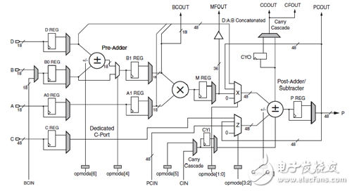
Figure 2-32 Detailed block diagram of DSP48A1
The M port is the 36-bit raw output of the multiplier. It can also be directly connected to the FPGA logic to accommodate multiple DSP operations.
The 18-bit D and B ports can be used as inputs to the 18-bit pre-adder, bypassing the pre-adder, or setting OPMODE[4] to connect the output of the pre-adder to the input of the multiplier.
The 18-bit A and B ports provide 18&TImes; 18 multiplier inputs, and D, A, and B can bypass the multiplier as an input to the X multiplexer. The 48-bit C port is used for the general input of the Z multiplexer to perform addition or subtraction.
The 25-bit and B-port 18-bit data of port A is 25 & TImes; 18 multiplier input. Each DSP48A1 can perform operations such as multiply, add, subtract, and so on. Ports A and B can be combined with a skip multiplier as an input to the X multiplexer.
The multiplexer is controlled by configuration bits to set the pass-through, register input, or cascade input of the signal. The data port registers are allowed to be used to balance the increase in clock frequency with the data delay. The pipeline register between the multiplier and the adder is the M register.
INMODE[3:0] is a new control bit in DSP48A1 that controls the functions of the A and D input registers and pre-adders.
(2) OPMODE port.
The OPMODE port (see Figure 2-33) supports two input modes, either through or through the register pipeline. Using the registration function, you can improve the performance of the DSP48A1.
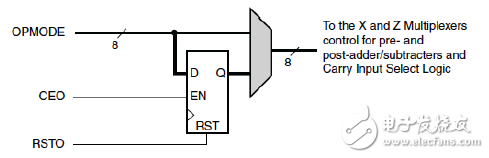
Figure 2-33 OPMODE port
(3) X and Z multiplexers.
OPMODE provides a way to dynamically change the function of the DSP48A1. The control bits of the OPMODE correspond to the selection bits of the X and Z multiplexers. The output of the multiplexer acts as the operand of the post-adder/subtractor.
(4) Carry input logic.
The carry input logic is a function of OPMODE[5] and CIN.
The possible carry inputs "converge" before the outputs of the X and Z multiplexers. In a sense, the X and Z multiplexer functions replicate the carry input signal to the carry logic.
OPMODE and CARRYINSEL must be set correctly to ensure proper selection of the carry input (CIN). There are two inputs in Figure 2-34. Select CIN or OPMODE[5] by the CARRYINSEL bit. CIN is the carry output of the upper DSP48A1, and OPMODE[5] is controlled by the FPGA logic.
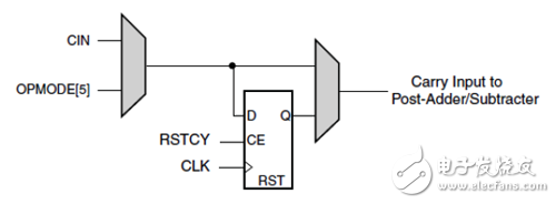
Figure 2-34 CARRYINSEL signal logic
Second, the arithmetic function(1) Pre-adder.
The output of the pre-adder/pre-subtractor is a function of the OPMODE[6] and B, D data. OPMODE[6] is defined as 1 for the subtraction operation.
(2) Multiplier.
As shown in Figure 2-35, the two's complement multiplier input is a two-bit complement of 18 bits, producing a 36-bit complement output. The output can be logically shifted to the right by 17 bits, concatenated into a wider number of multipliers.
By setting the highest bit of the input operand to 0, the multiplier can implement unsigned arithmetic.
The register MREG is the output register of the multiplier and can increase multiplier performance with a one clock cycle delay. The 36-bit output of the multiplier can be used as an input to the X multiplexer or connected to the internal logic of the FPGA via the M port (MFOUT[35:0]).
The 36-bit output of the multiplier can be sign extended to 48 bits as an input to the adder/subtracter.
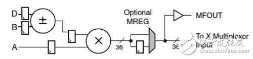
Figure 2-35 Multiplier in DSP48A1
(3) Adder/subtracter/accumulator.
The output of the adder/subtractor/accumulator is a function of OPMODE and input data. Which input is selected by the OPMODE[3:0] to the X/Z multiplexer, and then to the adder/subtractor/accumulator block .
The addition or subtraction operation is controlled by OPMODE[7], and OPMODE[7] is 1 for subtraction. The output of the X multiplexer is added to CIN, and the result is added/subtracted from the output of Z.
After analyzing the structure of DSP48A1, we know that it can be used to complete very complex DSP functions, such as FIR filters, which greatly improve the ability of digital processing.
The Xilinx tool provides primitives for DSP48 that can be instantiated in HDL, as shown in Figure 2-36. It can also be called through the Core Generator tool.
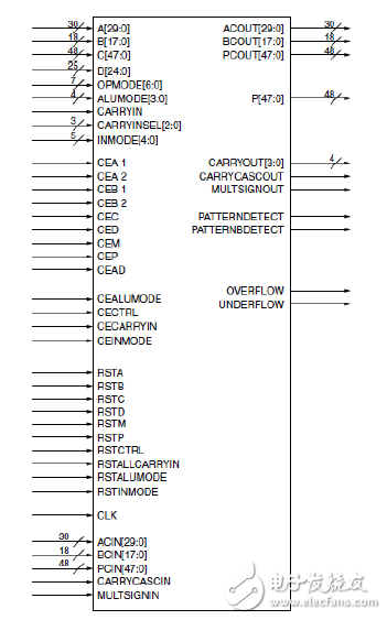
Figure 2-36 Primitives of DSP48
10W Medical Power Supply,Medical Device Adapter,Medical High Frequency Switch Power Supply,Multi-Parameter Monitor Power Supply
Shenzhen Longxc Power Supply Co., Ltd , https://www.longxcpower.com