Radio frequency (RF) and microwave amplifiers provide optimum performance under specific bias conditions. The quiescent current determined by the bias point affects the performance performance indicators such as linearity and efficiency. While some amplifiers are self-biased, many devices require external biasing and use multiple power supplies whose timing needs to be properly controlled to make the device safe to operate.
Next, we mainly talk about the bias timing control requirements.
Power sequencing
Power sequencing is very important when using an external bias amplifier for the following reasons:
1. Failure to follow proper power sequencing can affect device stability. Exceeding the breakdown voltage may cause the device to fail immediately. Long-term reliability is reduced when conditions exceeding the boundary conditions occur multiple times and the system is under pressure. In addition, continuous violations of the timing control mode can damage the on-chip protection circuitry and cause long-term damage, resulting in field operation failures.
2. Optimizing the bias level not only during power-up and power-down, but also during normal operation, can improve the performance of the RF amplifier, depending on configuration and application requirements. For some applications, the RF performance of the amplifier can be changed to suit different field conditions. For example, in rainy days, the output power can be increased to widen the coverage, and on a sunny day, the output power can be reduced. The amplifier's external gate voltage control enables these functions.
ADI has a wide range of RF amplifiers, many of which are based on depletion high electron mobility (pHEMT) technology. Transistors used in this process typically require a power supply to power the drain and gate pins. This quiescent drain current is related to the gate voltage.
See Figure 1 for typical IV characteristics of a typical field effect transistor (FET) process.
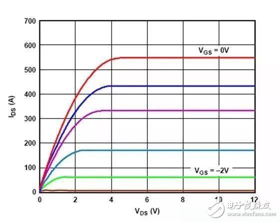
Figure 1. Typical IV characteristics of a typical FET process
As the gate-to-source voltage (VGS) increases, more electrons enter the channel, producing a higher drain-source current (IDS).
In addition, as the drain-source voltage (VDS) increases, the electric field force that pulls the electrons becomes larger, and the drain-source current also increases (in the linear interval).
In practical amplifiers, these amplifiers can be broadly classified into two categories due to effects such as channel length modulation: self-biased amplifiers and external bias amplifiers.
Self-bias amplifier
The self-bias amplifier has an internal circuit to set the optimum bias point for operation. These amplifiers are typically best suited for broadband low power applications. See Figure 2 for a typical pinout of a self-biased amplifier.
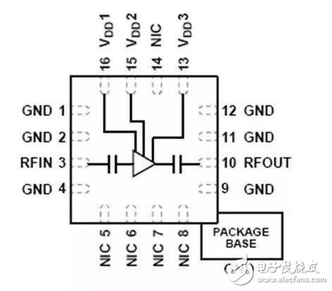
Figure 2. Typical pinout of a multistage self-biased amplifier with multiple bias pins
Self-biased amplifiers, while easy to use, may not provide optimal performance because internal resistive bias circuits do not adequately compensate for batch, device, and temperature differences.
External bias amplifier
External bias amplifiers often provide higher performance than self-biased amplifiers under certain bias conditions. The quiescent drain current of the amplifier affects parameters such as power compression point, gain, noise figure, intermodulation products, and efficiency. For these high-performance external bias amplifiers, proper power sequencing is critical to ensure that the device operates safely at peak performance.
Figure 3 shows a typical connection of the external bias amplifier pins and the corresponding transistor pins. The pin mapping in Figure 3 is a simplified schematic of the amplifier.
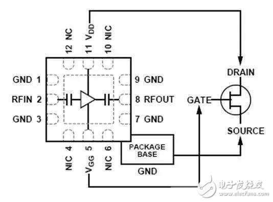
Figure 3. Typical connection of an external bias amplifier
In addition, many external bias amplifiers meet multiple gain, bandwidth, and power requirements through multiple stages. Figure 4 shows a typical block diagram of the multi-stage external bias amplifier HMC1131.
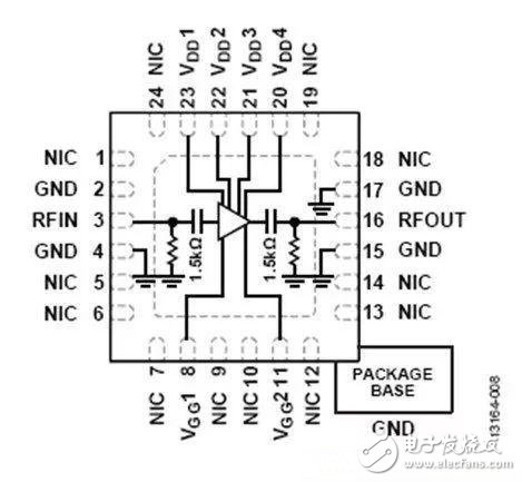
Figure 4. HMC1131 Multistage External Bias Amplifier
Give a chestnut: timing and control requirements for an external bias amplifier
The HMC1131 is a power amplifier for gallium arsenide (GaAs), pHEMT monolithic microwave integrated circuits (MMICs). The operating frequency range is from 24 GHz to 35 GHz. The typical performance offered by this 4-stage design is 22 dB gain, 23 dBm output power (1 dB compression, or P1dB) and 27 dBm saturated output power (PSAT). The corresponding bias conditions are VDD = 5 V and IDQ = 225 mA. Where VDD is the drain bias voltage and IDQ is the quiescent drain current. This information is given in the HMC1131 data sheet for the electrical specification table for the 24 GHz to 27 GHz frequency range. Figure 4 shows the pin connections for the HMC1131.
To achieve a target quiescent drain current (IDQ) of 225 mA, the gate bias pin voltages (VGG1 and VGG2) should be set between 0 V and −2 V. To set this negative voltage without damaging the amplifier, follow the recommended bias sequence during power-up and power-down.
The following is the recommended offset sequence during power-up of the HMC1131:
Connect to ground to set VGG1 and VGG2 to −2 V Set drain voltage bias pins VDD1 to VDD4 to 5 V Increase VGG1 and VGG2 to achieve 225 mA IDQ Apply RF signalThe following is a recommended offset sequence during the HMC1131 power down:
Turn off the RF signal and lower VGG1 and VGG2 to −2 V to achieve an IDQ of approximately 0 mA. Reduce VDD1 to VDD4 to 0 V. Increase VGG1 and VGG2 to 0 V.When the gate voltage (VGGx) is −2 V, the transistor is pinched off. Therefore, the typical value of IDQ is close to zero.
Front Serviceable Cabinets UHD led screen video wall P1.25, P1.56 P1.875, P1.923 and P2.5
Small pixel pitchled screen cabinet design that will forever change the way LED video displays are specified. Feature for feature, HD, 4K, or 8K. This series of LED diplays screens are designed for Broadcasting, Control Room and 24/7 Emergency Operation Center applications, featuring redundant power supply and receiving card. These features will provide a worry free video display for mission critical applications.
Compare with LCD sets, indoor led video wall has many advantages.That's why the UHD led display are getting more and more popular and acceptable
Small Pixel Pitch Led Display, Small Pixel Pitch Led screen ,UHD Led Screen UHD led display ,Small Pixel Pitch Led Video Wall
Shenzhen Priva Tech Co., Ltd. , https://www.privaled.com