For better clock control, the Virtex-6 device is divided into several clock regions, the smallest device has six regions, and the largest device has 18 regions. Each clock area is 40 CLB high. In clock design, it is recommended to use on-chip dedicated clock resources. Local clocks (such as logic-generated clocks) are not recommended.
The middle column of each Virtex-6 contains a dedicated configuration pin (CFG) and the rest of the column is CLB. A CMT column is arranged on the right side. Each zone (40 CLB high) corresponds to one CMT. A CMT contains 2 Mixed Mode Clock Management Units (MMCMs) and 32 vertical global clock trees. There is one clock line (HROW) in the middle of each clock region, including 12 horizontal clock lines, 6 BUFRs, and up to 12 BUFHs. The clock resource diagram of Virtex-6 is shown in Figure 5-7.
There is one I/O column on each of the left and right sides of each Virtex-6 FPGA middle column, labeled IOCL and IOCR, and CLB between the I/O column and the middle column.
There is one horizontal clock line (HROW) in the middle of each area /BANK, and HROW contains horizontal clock lines, BUFG and BUFH. The internal I/O column contains eight global clock pin pairs (GC), and all I/O columns contain four Clock-Capable pin pairs (CC) that can be connected to BUFIO and BUFR. Two of the four CCs of each BANK can be connected to the BUFIO of the adjacent area. In addition, the BUFR and CC pins of the middle column can directly drive the MMCM of the same area, or indirectly drive the BUFG through the vertical global clock line.
The on-chip clock resource of the Virtex-6 device provides clocks for on-chip synchronization components. There are three types of on-chip clock resources, namely global clock resources, regional clock resources, and I/O clock resources.
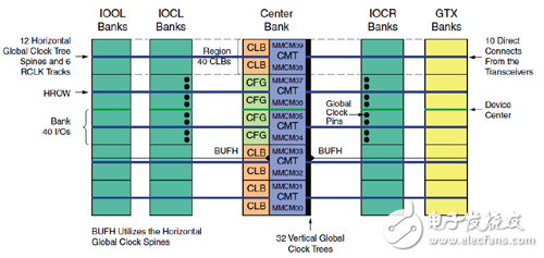
Figure 5-7 Virtex-6 clock resource diagram
First, the global clock resourcesThe global clock is a dedicated interconnect network that reduces clock skew, duty cycle distortion, and power consumption to increase jitter tolerance.
Virtex-6's global clock resources are designed with a dedicated clock buffer and driver structure to minimize the global clock's latency to CLB, IOB, and BRAM.
The global clock resource consists of the following paths and components.
Second, the global clock inputThe Virtex-6 global clock input contains dedicated global clock input pins and global input buffers. The global clock input pin can be directly connected to an external single-ended or differential clock; the global input buffer (IBUFG) is the first-level global buffer inside the FPGA that is connected to the dedicated global clock input pin.
There are eight global clock inputs in the Virtex-6 device. Eight global clock inputs can be connected to eight clock inputs on the board.
The clock input pin can be used as a normal I/O instead of as a clock input pin.
An external single-ended or differential clock enters the FPGA through a dedicated global clock input pin. Within the FPGA, the signal must be connected to the global input buffer (IBUFG), otherwise an error will be reported during placement and routing.
The global input buffer can be instantiated in the HDL code.
(1) Global clock buffer.
Each Virtex-6 device has 32 global clock buffers, and the clock signal can only drive the global clock network after passing through the BUFG. A global clock input can be connected directly from the P terminal of the differential global clock pin pair to the input of the global clock buffer. Each differential global clock pin pair can be connected to a differential or single-ended clock on the PCB. If a single-ended clock is used, the P terminal of the pin pair must be used because there is only a direct connection on this pin. A single-ended clock must be connected to the positive (P) terminal of the differential global clock pin. If a single-ended clock is connected to the P terminal of a differential pin pair, its N-side cannot be used as another single-ended clock input. However, it can be used as a normal I/O.
The input sources of the global clock buffer include the following.
Global clock input.
The same area of ​​the internal I/O column, the Clock-Capable clock input.
Clock Management Unit (CMT).
Output of other global clock buffers (BUFG).
General purpose interconnection.
Area Clock Buffer (BUFR).
Gigabit transceiver.
The CC input of the Virtex-6 FPGA drives the BUFG indirectly through the vertical clock network in the MMCM column. The 32 BUFGs are divided into two groups of 16 each located at the top and bottom of the device. The top MMCM can only drive the top 16 BUFGs, and the bottom MMCM can only drive the bottom BUFG.
The global clock buffer can also be configured as a multiplexer that can be switched between 2 input clocks. The two clocks can be either synchronous or asynchronous, and the output of the multiplexer is a glitch-free clock.
The various primitive models of the global clock buffer are shown in Table 5-6.
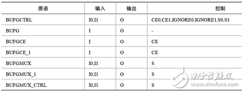
Table 5-6 Primitives of the global clock buffer
(2) Global clock tree and clock network (GCLK).
The global clock tree and clock network in Virtex-6, if not used, is disconnected, which reduces power consumption. In addition, the clock tree also has a management function for load/fanout. All global clock lines and buffers are implemented differentially, which helps improve duty cycle and improve rejection of common mode noise. In the Virtex-6 architecture, the global clock line can be used not only as a clock, but also as other signal lines, such as fanning out larger signals.
(3) Clock area.
Galanz Microwave Oven Panel Membrane Switch
Microwave steam can be used in all kinds of food, the microwave oven before use the switch is the rotary switch, no food set, only by rotating for temperature adjustment, some people think that is very convenient, but the time is progressive, meet now microwave Membrane Switch, you will know a rotary switch is already obsolete. There are different patterns and different temperatures set on the membrane switch. The pattern is usually the pattern of food, so the pattern can be selected according to the different steamed food, and each pattern is also involved in the temperature, so as long as the pattern is selected, the temperature can be directly regulated systematically. Automated products bring more convenience to people, and the temperature and time can be displayed autonomously on the membrane switch.
Galanz Microwave Oven Panel Membrane Switch,Balances Membrane Switch,Analytical Balances Membrane Switch,Gloss Surface Membrane Keypad
Dongguan Nanhuang Industry Co., Ltd , https://www.soushine-nanhuang.com