Experiment on the xilinx ZC7020 film;
[in conclusion]
Ordinary IO cannot be directly used as the clock input of the PLL, and the dedicated clock pin can be used;
Ordinary IO can be connected to the clock input of the PLL through BUFG, but to change the setting of the PLL setting input clk, select "No Buffer";
Specific internal layout assignments can be viewed through Xilinx's FPGA Editor.
The clock management of ZYNQ is also slightly different from the previous one, and then introduced in another article, related documents.
[Demo1]
// demo1 two bufg connect
Module iobuf(
Input clk,
Input rst,
Output led
);
Wire clkin_w;
BUFG BUFG_inst (
.O(clkin_w), // Clock buffer output
.I(clk) // Clock buffer input
);
Pll0 u_pll0(
.CLK_IN1(clkin_w), // IN
.CLK_OUT1(clkout), // OUT
.RESET(rst)); // IN
Assign led = clkout;
Endmodule
The default input front end of the phase-locked loop PLL has a BUFG unit, and the two BUFGs cannot be connected, so this error is reported:
ERROR: NgdBuild: 770 - IBUFG 'u_pll0/clkin1_buf' and BUFG 'BUFG_inst' on net
'clkin_w' are lined up in series. Buffers of the same direcTIon cannot be
Placed in series.
ERROR: NgdBuild: 924 - input pad net 'clkin_w' is driving non-buffer primiTIves:
[Demo2]
// demo2 regular io directly connect to PLL
Module iobuf(
Input clk,
Input rst,
Output led
);
Wire clkin_w;
/*
BUFG BUFG_inst (
.O(clkin_w), // Clock buffer output
.I(clk) // Clock buffer input
);
*/
Pll0 u_pll0(
.CLK_IN1(clk), // IN
.CLK_OUT1(clkout), // OUT
.RESET(rst)); // IN
Assign led = clkout;
Endmodule
Ordinary IO can't directly input the phase-locked loop, so it will report such a mistake:
ERROR: Place: 1397 - A clock IOB / MMCM clock component pair have been found that
Are not placed at an opTImal clock IOB / MMCM site pair. The clock IOB
Component is placed at site . The corresponding MMCM component
Is placed at site . The clock IO can
Use the fast path between the IOB and the MMCM if the IOB is placed on a
Clock Capable IOB site that has dedicated fast path to MMCM sites within the
Same clock region. You may want to analyze why this problem exists and
Correct it. If this sub opTImal condition is acceptable for this design, you
May use the CLOCK_DEDICATED_ROUTE constraint in the .ucf file to demote this
Message to a WARNING and allow your design to continue. However, the use of
This override is highly discouraged as it may lead to very poor timing
Results. It is recommended that this error condition be corrected in the
Design. A list of all the COMP.PINs used in this clock placement rule is
ERROR:Pack:1654 - The timing-driven placement phase encountered an error.
If there is a constraint in ucf:
NET clk CLOCK_DEDICATED_ROUTE = FALSE;
Still will report an error, in the ZYNQ7000 series, this is still not passed, as follows:
ERROR: PhysDesignRules: 2256 - Unsupported MMCME2_ADV configuration. The signal
U_pll0/clkin1 on the CLKIN1 pin of MMCME2_ADV comp u_pll0/mmcm_adv_inst with
COMPENSATION mode ZHOLD must be driven by a clock capable IOB.
ERROR:Pack:1642 - Errors in physical DRC.
Use normal IO, then connect bufg to connect to the clock line.
This error will still be reported, because the two bufg are still connected:
ERROR: NgdBuild: 770 - IBUFG 'u_pll0/clkin1_buf' and BUFG 'BUFG_inst' on net
'clkin_w' are lined up in series. Buffers of the same direction cannot be
Placed in series.
ERROR: NgdBuild: 924 - input pad net 'clkin_w' is driving non-buffer primitives:
[Demo3]
// dem3 regular io with BUFG then connect to PLL which with "No Buffer" setting
Module iobuf(
Input clk,
Input rst,
Output led
);
Wire clkin_w;
BUFG BUFG_inst (
.O(clkin_w), // Clock buffer output
.I(clk) // Clock buffer input
);
Pll0 u_pll0(
.CLK_IN1(clkin_w), // IN
.CLK_OUT1(clkout), // OUT
.RESET(rst)); // IN
Assign led = clkout;
Endmodule
The PLL settings are as shown below.
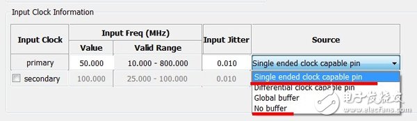
In this way, the normal IO can be used as the clock input of the PLL, and the bit is generated smoothly;
The clock is still best to use the global clock IO, you must pay attention when drawing:)
There is no concept of global clock in zc702, but there are a lot of dedicated clock pins, which are the same;
| About Paper Covered Wire. |
Paper Covered Wire includes NOMEX Coated Copper Wire, Paper Covered Flat Aluminium Wire, Paper Covered Flat Copper Wire.
Application: oil-immersed transformer windings
Using 100% oxygen free pole as extrusion raw material, insulation material using high density telephone paper, cable paper, polyester, non-woven fabric.Self-locking wrapping is adopted within 6 layers, the bending performance is 15% higher than the national standard, the temperature index is 105℃ after the phone paper and cable paper are impregnated, this product has excellent voltage resistance performance in oil, widely used in transformer coil, stable performance, short processing cycle.

As per Conductor Material:Copper , aluminum
As per Inner Conductor: Paper wrapped bare
Insulation thickness:Double paper covered (DPC) or Triple Paper Covered (TPC) ,According to Customer`s requirements
Insulated Wire Copper,Paper Covered Wire,Paper Covered Copper Flat Wire,Paper Covered Insulated Wire Copper
HENAN HUAYANG ELECTRICAL TECHNOLOGY GROUP CO.,LTD , https://www.huaonwire.com