Non-synchronous, boost, and power conversion topologies are often used in applications such as LED drivers. In these applications, the input voltage (VIN) is not sufficient to forward bias a set of series/parallel LED strings. This inductive switching topology generates the compliance voltage necessary to achieve LED current regulation and is commonly used in LCD backlight applications. For example, in LED matrix applications such as automotive interior and exterior lighting away from the driver, catastrophic consequences can occur if there is a risk of shorting the output to ground. Limiting the current and running the protection circuit as an electronic circuit breaker can prevent these catastrophic failures.
As shown in Figure 1, the input of the boost converter is physically connected to its output through a boost inductor (L1) and a boost diode (D1). Therefore, a short circuit condition on the output saturates the boost inductor, which causes a current spike sufficient to damage the boost diode. Worse, this short circuit can also interfere with all devices connected to the input, including pulse width modulation (PWM) controllers. Obviously, some type of circuit protection is needed to power remote LEDs when using this topology. Next, consider designing a versatile, low-cost circuit that can be optimized to protect the boost converter and prevent short-circuit loads at the input. In addition, we will verify the required response through an analog circuit.
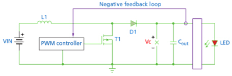
Figure 1. LED driver circuit based on non-isolated boost topology
Current limiter and electronic circuit breaker
The Shunt Monitor (CSM) is a high precision, high gain differential current sense amplifier that is often used to monitor input and output currents. Figure 2 shows its typical configuration. This particular device integrates an open-drain comparator; this comparator can be set to toggle, latch, and reset on pre-set line currents.
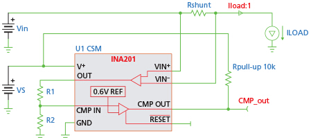
Figure 2. A shunt monitor component adds protection
The output of this comparator can be used to control an external MOSFET switch that can interrupt the load short circuit within a few milliseconds. In addition to interrupting the input current when a fault condition occurs on the output, the analog output can also solve the so-called "negative input impedance" problem of the switching regulator, preventing the input current from increasing with decreasing input voltage.
The input is clamped by connecting the input current to the output current in a logical "OR" configuration. As shown in Figure 3, the purpose is to generate a composite feedback signal that drives the PWM controller. The CSM then disables the output current feedback and forces the LED current to decrease as the input voltage drops below a preset level, limiting the input current.
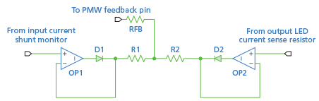
Figure 3. Input current limiter relies on sense input and output current
Circuit operation
Figure 4 shows the circuit implementation of a boost converter LED driver with output short-circuit protection. The LEDs produced by Osram Opto Semiconductors Ostar in the circuit are a device for automotive headlamp applications, actually a single piece, LED on an insulated metal substrate. This device has a surge current rated at 2A (less than 10 μs) and a typical forward voltage of 18V at 1A. The DC/DC boost converter senses the forward LED current on the feedback pin and fully adjusts the output voltage to regulate the LED current. The LED current is set by the sense resistor (RSNS) and its value is proportional to the internal bandgap reference of the PWM converter (RSNS = VREF/ILED). Using a boost converter with a low reference makes it easier to achieve higher converter efficiency and reduce component thermal stress.
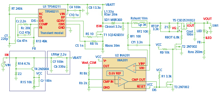
Figure 4. LED boost driver circuit with shorted load fault protection
Although the lifetime can be as long as 50,000 hours or more, LEDs are very sensitive to temperature and electrical overstress, and their dynamic impedance characteristics often pose challenges for the selection of switching regulator components and the design of control loops. These selections and design challenges are described in this operating manual. In this way, the circuit simulation shown in Figure 4 was developed to analyze the complexity of the LED driver/protection circuit and predict the operation of the circuit under various operating conditions.
The PWM controller selected for this analysis has a feedback reference voltage of 0.26V. Therefore, when the LED current is 1A, the power dissipation of the LED sensing resistor is only 0.26W. Since the CSM has a gain of 50, a much smaller sense resistor is needed to sense the output current. When the current flowing through the CSM shunt resistor exceeds the limit set by the CSM sense resistor, the CSM gain and the comparator threshold (R, R), the PMOS turn-on transistor interrupts the load current - thereby acting as an electronic circuit breaker .
The latched output can be reset by switching the RESET pin low. However, for the purposes of this article, RESET has been disabled to verify response speed. The response speed and peak current depend on many variables. These variables include component selection, CSM bandwidth, noise filter, output capacitor, FET selection, and output boost inductor. These factors together affect the output impedance of the converter. In order to accurately evaluate the mode of operation, we have run the simulation with a maximum time step of 50 ns and a DC relative tolerance set to 0.001%. This analysis runs in TINA-TI, a free Berkeley SPICE 3f5 compatible emulator. The 5ms simulation of the boost converter with a working frequency of 300kHz can be started to a steady state in just 30 seconds.
Where is the CSM placed?
The CSM can be placed on the input or output of the boost converter. In this simulation, the CSM is placed on the output, which senses the current through a 10 mΩ shunt resistor in parallel with the output PMOS pass element (T5). This circuit prevents internal and/or external short circuit conditions depending on where the CSM is placed. However, the CSM must be designed to have a sufficient common mode range (CMR) under all operating conditions.
If placed on the input of the boost converter, a CSM with a lower CMR can be selected. However, placing the CSM on the output avoids the boost inductor and helps speed up the reaction time for short-circuit conditions. Regardless of where the CSM is placed, an RC filter should be used to attenuate noise and resonant ringing that can occur due to sudden di/dt events of the shunt resistor. A small 100 resistor and differential capacitor can be placed into a time constant that is three times larger than the estimated shunt Lp/R time constant, where Lp is the parasitic shunt inductance. Since the gain error and bandwidth of the CSM are negatively affected by the noise filter, it is important to keep the low value of the filter.
Simulation result
Figure 5 shows the simulation results. Vg is the control voltage to the PMOS FET and is normally set to -6V. It needs to be optimized based on the threshold voltage, gate charge, and saturation characteristics of the FET. Minimizing the voltage on the gate improves reaction time and pull-up resistors should be chosen to minimize the interruption period. It should be noted that the input current and gate voltage are shown with high gate charge (purple) and low gate charge (blue) MOSFET.
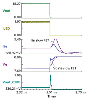
Figure 5. Standard wired and wireless networks will carry relatively simple commands and data between physical building systems and building management equipment.
It is clear that lower gate charge devices minimize the visible current on the input. Selecting the MOSFET and gate drive circuitry for optimal response is a very important design consideration because it limits the di/dt and meets the safe operation of the MOSFET. These complex design considerations are not so easy to analyze; therefore, it is best to simulate and validate them on the bench.
Special test software is provided on some oscilloscopes such as Tektronix products to calculate the switching power loss relative to the safe operating curve of the MOSFET. This simulation suggests a response duration of less than 2μs, which results in less than 6A of input current before the current is interrupted. The choice of interrupt FET will affect the peak input and output current. A high-performance, hot-swappable controller that drives high-end NMOS devices is another option and can achieve interrupt times of less than 250ns. These devices are optimized for backplane hot-swap card insertion, but can provide a higher performance solution than the one shown here.
Avoided failure
This circuit demonstrates and mimics the interrupt scenario and limits the input/output current of the boost converter LED driver under varying load conditions. The circuit is optimized for automotive LED headlamp driver applications. We demonstrate that careful analysis and component selection are required to achieve optimal circuit response times. Integrating these sensitivities into a comprehensive time domain circuit simulation helps to understand the circuit operating conditions for different operating conditions and component selections.
Specialized hot-swappable controllers are available with specialized features and optimized performance that should be taken into account when designing. In either case, careful analysis is necessary when executing a circuit to interrupt or limit the power supply. Designing a robust and robust protection circuit for LED drivers is a complex task, and software tools such as TINA-TI, SPICE, and WEBENCH can help with faster analysis and design.
Author: John Rice, Texas Instruments (TI) Power Systems Engineer
Traffic Lights are traffic lights that command traffic and are generally made up of red lights,green lights and yellow lights.The red light means no traffic,the green light is allowed to pass,and the yellow light is a warning.
Traffic lights are divided into:light motor vehicles, no-motor vehicles lights,pedestrian signal lights,direction indicator lamp(arrow lights),driveway lights,flashing warning lights,road and rail light plane crossing.
Traffic Lights
Traffic Lights,Traffic Lights For Sale,Traffic Lights Word Search,Traffic Lights Invented
Jiangsu chengxu Electric Group Co., Ltd , https://www.chengxulighting.com