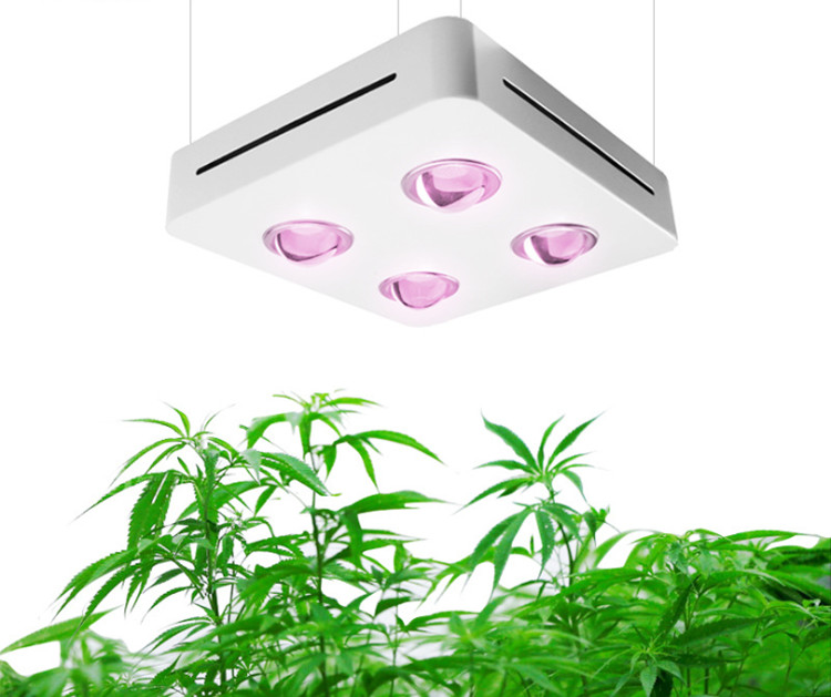
COB package challenges outdoor small pitch new limit SMD package will face huge challenges

COB packaging has gradually matured in the field of LED display applications, especially in the field of outdoor small pitch, with its unique technological advantages, it has already broken through the outdoor P3.0 level, and it is inevitable to break through the outdoor P2.0 level in the near future. . So where is the COB packaging technology sacred? Why is there such a fierce performance when one angstrom appears, which is impressive? Where is its technical advantage?
one. What is a COB package?
The English word for COB package is Chip On Board. The literal translation is that the chip is placed on the board. as the picture shows
COB package
In the field of LED display technology, the COB packaging process is to fix the LED bare chip with conductive adhesive or insulating glue on the lamp position pad of the PCB, and then use the ultrasonic welding technology to conduct conductive function wire bonding of the LED chip , and finally use epoxy. The resin glue encapsulates the lamp position to protect the LED light-emitting chip.
2. The difference between the COB packaging process and the DIP and SMD packaging processes.
as the picture shows:
DIP package
DIP package
SMD package
SMD package
The DIP and SMD packaging processes are indistinguishable from COB packages in terms of bond wires, the biggest difference being the use of brackets in the red section. As we all know, the bracket has four soldering legs that need to be soldered to the PCB via SMT. Therefore, the biggest difference between the COB packaging process and the DIP and SMD packaging processes is that a lamp surface over-reflow soldering process is eliminated.
III. Advantages of the COB packaging process
High reliability
An important indicator for evaluating reliability is the dead light rate:
The national standard currently used in the LED display industry is: three ten thousandths
The COB packaging process enables this indicator to achieve:
Full color screen: less than five hundred thousandths
Single and dual color screen: less than 8 parts per million
Why the COB package display has such high reliability, we analyze it through the following five points:
A: The control of the single lamp production process is reduced.
Everyone knows that a full-color lamp bead requires five wire bonds.
as the picture shows
Full color lamp beads
The COB packaging process only needs to control the quality of the five bonding wires in the production process, and the SMD process needs to control the quality of the five bonding wires, and also needs to control the welding of the four soldering legs of the bracket when the lamp surface is over the reflow soldering process. Quality, as shown:
According to the reliability principle, the fewer the control links of a system, the higher the reliability. The control links for COB and SMD are 5 and 9, respectively, so the reliability of SMD is at least double that of COB in this respect.
Look at the picture below:
If you produce 1 square meter of P10, the SMD packaging process will have an additional 40,000 control points. If the dot density is doubled, that is, the dot density reaches the P5 level, the SMD packaging process requires 160,000 solder joints per square meter to be controlled. If the dot density is further reduced to the P2 level, the SMD packaging process requires 1 million solder joints per square meter to be controlled. How to ensure that 1 million solder joints do not have false soldering, continuous soldering, and virtual soldering in the case of P2 small dot spacing is a very difficult problem.
The COB packaging process created a revolutionary step that eliminated the bracket welding process.
B. COB eliminates the need to reflow the lamp bead surface, and there is no microscopic damage to the LED chip and wire bond caused by high temperature in the reflow oven.
The SMD lamp bead needs to be surface-welded to solder it to the PCB. Therefore, it must withstand the temperature of 240 ° in the furnace. If the TG point of the epoxy resin is too low, the high temperature will cause the thermal expansion coefficient of the colloid to increase sharply. The destruction of the LED chip bonding wire is invalid. In addition, the high temperature is transmitted through the holder pins to the chip, which increases the possibility of crystal chipping failure.
C. The COB packaging process directly fixes the LED bare chip to the pad, so the heat dissipation area is larger than the SMD, the heat transfer coefficient is also high, and the heat dissipation is good.
SMD is to fix the LED bare chip on the pad inside the bracket. The pad needs to transfer heat to the PCB through the bracket metal pin.
D. COB packaging process circuit board adopts the sinking gold process, and there is no PCB board tin-spraying process using SMD package, so the PCB board line has high oxidation resistance.
E. COB packaging process lamp surface curve is smooth and hemispherical, as shown:
COB packaging process lamp surface curve is smooth and hemispherical
The SMD has a quadrangular shape with obvious edges and corners. In the subsequent outdoor nano-coating, anti-ultraviolet coating and three-proof paint spraying outdoor protection treatment process, COB has no shadow area and no dead angle. SMD, on the outdoor protection of the four-leg or six-leg pads of the surface-mounted lamp beads, will face a huge challenge in how to deal with the antioxidant capacity of these millions of solder joints.
2. Provincial cost
Compared with the SMD packaging process, the COB packaging process saves costs, mainly from the following four aspects:
A. Saving raw material costs
Metal materials such as brackets and braids are no longer used in COB packaging.
B. Saving process cost
The COB package saves the cutting, splitting, braiding and reflow soldering of the lamp bezel.
C. Save on transportation costs
The COB package no longer uses a bracket, saving the weight of the bracket. For example, a square meter SMD P3 full color screen will use 111111 brackets.
The COB package uses a point-by-point precision dispensing process to protect the bare LED chip, so the amount of glue used is very small. Taking P3 full color as an example, a module with 1024 lamp beads uses less than 3 grams of glue. Therefore, the weight of the module is also saved.
Saving on weight saves logistics costs.
D. Simplified production organization process
The COB packaging process integrates the production process of the middle and downstream enterprises of the LED display industry chain, and can complete the manufacturing process from LED lamp bead packaging to LED display in one enterprise, saving production organization cost, intermediate link packaging and Logistics costs, quality control costs, etc.
The SMD packaging process is done by the lamp bead packaging factory, and the packaging is transported to the LED display production enterprise.
3. Easy to achieve small dot spacing
For the application trend of small dot pitch, it is possible to break through the P1.0 level in the future. If the reliability is concerned, the advantages of the COB packaging process are much stronger than the SMD packaging process for the following reasons.
Take the P1.0 level as an example: the point density per square meter P1.0 is calculated as follows:
1÷(0.001X0.001)=1000000
For 1 million points, with 4 brackets for each point, the entire production process needs to control 4 million solder fillets, which is very difficult, and the COB package will not have this difficulty, so it is reliable. Sex is much higher than SMD.
Also, the COB package is no longer limited by the size of the bracket when designing the diameter of the lamp, as shown in the following figure:
The COB package is no longer limited by the size of the bracket when designing the diameter of the lamp bead.
The current technology can design the diameter of the lamp bead to 1.2mm, and the safety distance between the lamp bead and the lamp bead can reach 0.5mm. Theoretically, the dot pitch can achieve the P1.7 level. In the future, with the advancement of LED chip technology, the size is further reduced, or there is the emergence of flip-chip LED chips. Breaking through the P1.0 level is no longer a dream.
4. Light and thin 180° large viewing angle is easy to bend
A. Light and thin:
The weight of the COB package module is 1/2 lighter than the weight of the SMD package module.
Thin and light
Compared with the outdoor module with the same point density, the COB module is about 10kg lighter per square meter than the SMD module.
B. 180° large viewing angle
Since the COB package uses a hemispherical lens to illuminate without a cover, the theoretical illumination angle can reach 180°.
SMD is generally at 125° and can reach a maximum of 160°.
C. Flexible
Since the COB package has no bracket soldering, the LED chip is sealed in the lamp position by the epoxy resin, so it can be bent arbitrarily. The bending ability is determined by the size of the module and the thickness of the PCB. The SMD module is not able to bend.
Flexible
5. Pressure resistance, impact resistance, easy to clean
A. Compression, impact resistance, wear resistance
The lamp position of the COB module is encapsulated with epoxy resin. The high TG point glue has good physical properties as follows:
Compressive strength: 8.4kg/mm2
Shear strength: 4.2kg/mm2
Impact strength: 6.8kg*cm/cm2
Hardness: Shore D 84
Take the P4 lamp bead as an example: the diameter of the lamp bead is D=2.8mm
The lamp bead package area is: S=Ï€r2=3.14X1.42=6.15mm2
The pressure of a single lamp bead is: 6.15X8.4=51.66kg
The lateral shear force of a single lamp bead is: 6.15X4.2=25.83kg
B. Easy to clean
Since the mask of the COB module light board is no longer used, it can be directly washed with water after being used for a period of time outdoors.
four. in conclusion
In the future application of small-pitch LED display products, SMD will face enormous challenges in terms of reliability, achieving smaller spacing, and cost. The COB package has revolutionized its breakthrough and has eliminated the burden of the bracket. Lightly moving forward, the future is bright. The development of the future technology must be six feet, but not four feet.

Contain Grow Light Cob Waterproof 50w,100w and 150w,  Grow Light Cob ,COB Led Grow Light Diy. Cob Grow Lights use high power Epistar chip, with high par value, 4000k white lighting/pink lighting avaible.

Led Cob Chip Grow Light works well for plant growth, 50w can replace hps 300w, 100w can replace 500w, 150w replace 1000W Led Grow Light .

Features:

1.Waterproof IP67, works safely outside;

2.Driverless, no noise;

3.Light weight and small size, can save your shipping cost.

Waterproof  grow light Cob :
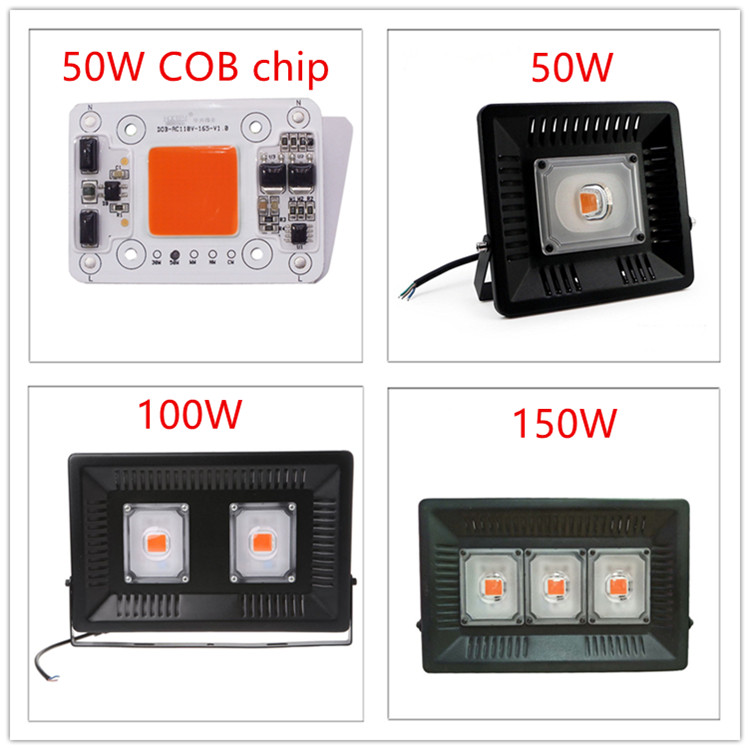
Grow Light Cob Diy

Diy Grow Light cob:

Diy Grow Light


COB Grow Light Series

Cob Led Grow Light,Led Cob Full Spectrum ,Diy Cob Led Grow Light ,Led Cob Grow Light

Shenzhen Wenyi Lighting Technology Co., Ltd , https://www.wycngrow.com