
With the development of computer science and automatic control technology, more and more different kinds of intelligent robots appear in factories and life. As an important subsystem in intelligent robot systems, robot vision system is getting more and more people's attention. . It covers areas such as image processing, pattern recognition and visual tracking. Different types of robots have different priorities because of their different work, and their visual systems have subtle differences in software or hardware. This paper studies the monocular vision system based on service robots. It deals with two-dimensional images based on the recognition of the color and shape of unobstructed objects and the translational tracking of 3D target objects.
The visual system is a very complex system. It not only needs accurate image acquisition but also real-time response to external changes. It also needs real-time tracking of external motion targets. Therefore, the vision system puts high demands on both hardware and software systems. At present, the popular soccer robot technology, its visual system belongs to the typical type of rapid recognition and reaction. In general, it uses the method of color mark calibration to achieve the recognition of players and targets, and the tracking function of the target is achieved by extending the prediction function of the Kalman filter. In hardware, an off-the-shelf camera is used to implement an image acquisition system for a robot.
The system adopts CMOS image sensor instead of CCD type sensor for image acquisition, DSP processing chip TMS320VC5509A for image processing and CPU control. In the design process, in order to visualize the effect of robot vision system recognition and tracking, a special one is adopted. LCD in LCD format for visual display. In software, part of the soccer robot's visual technology is used to achieve fast recognition of the target, and the Jacobian matrix constructed by the global feature moment achieves adaptive tracking of the target.
1 hardware part design
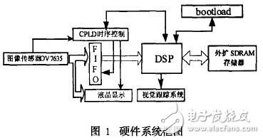
Figure 1 is a functional block diagram of the system hardware circuit.
1.1 Image Acquisition
The visual lens images the external image information on the area array unit of the image sensor. Currently popular image sensors include a CCD (Charged Coupled Device) type and an area array CMOS. Compared with the CCD type image sensor, the active pixel unit of the CMOS image sensor provides an amplifier for each pixel, requiring only a single supply of low logic level voltage, and the power consumption is only one tenth of that of the CCD. The CMOS image sensor integrates an A/D conversion section to directly output digital signals. Based on these factors, the system uses Omnivision's CMOS color image sensor OV7635.
The resolution of the OV7635 is 640X480, which can output 8-bit data in 3 formats: YCbCr4: 2:2 mode, RGB4:2:2 mode and RGB raw data mode. The output VGA format can be up to 30fps (fps: frames per second). Can work under progressive scan and interlaced scan. The OV7635 has two modes of operation, master mode and slave mode. In master mode, the sync signal and clock are not controlled by the peripheral device. In the slave mode, the field sync signal VSYNC of the OV7635, the line sync signal HREF, and the crystal oscillator frequency XCLK of the system are all controlled by an external device. This system uses the main mode. The OV7635 configures the on-chip registers via the I2C bus to output raw data. After the system power-on reset, the CMOS registers are initialized by the I2C bus signal of the DSP chip. The OV7635 then outputs the image signal as required. The line sync signal HREF, the field sync signal VSYNC, the pixel clock signal PCLK, and the digital image signal are included.
1.2 LCD display
In order to visually see the visual system's recognition and tracking effect, a PT035TN01 LCD screen from INNOLUX was used. In order not to increase the burden on the DSP, but also to see the tracking effect on the external target object in real time, the data of the liquid crystal display is directly displayed through the image data signal output by the sensor OV7635 and the CPLD control timing without passing through the DSP. PT035TN01 is a 3.5-inch TFT format LCD with resolution of 320 & TImes; 3 (RGB) & TImes; 240, LCD IF1, IF2 two input control pins to select the input data format: serial RGB format, CCIR601 format, CCIR656 format. There are four types of liquid crystal scanning modes. The input data format adopted by the vision system is CCIR601 format, and the scan mode is a scan mode from top to bottom and left to right.
In the CCIR601 format, the pixel clock PCLK output by the image sensor is divided by the CPLD as the operating clock of the liquid crystal, and the line sync signal HREF output by the image sensor is processed by the CPLD as the line sync signal HIS of the liquid crystal, thus, under the control of the CPLD. The data signal output by the image sensor OV7635 is sent to the liquid crystal for display.
1.3 Timing Control
The field sync signal VSYNC, the line sync signal HREF and the pixel clock signal PCLK outputted by the OV7635 are connected to the CPLD chip, and generate a control signal to store the data signal output by the OV7635 in the FIFO frame memory AL422B, and generate a liquid crystal clock and a line sync signal to control the liquid crystal. Display. CPLD uses ALTERA's EPM7064 chip. In the CPLD, functions such as write control to the FIFO, notification of the DSP read signal, and generation of the clock signal of the liquid crystal are completed.
The CPLD receives the field sync signal VSYNC. The falling edge of this signal indicates the beginning of a frame output by the image sensor. At this time, the CPLD generates a WRST negative pulse reset FIFO write pointer. After the falling edge of the field sync signal VSYNC, it is judged that the rising edge of the line sync signal HREF arrives, and then the image data is directly stored into the FIFO by using the pixel clock signal PCLK as the write clock WCK, and when a certain number is stored, the signal is sent to the FIFO in time. DSP, so that the DSP reads the data, the system uses an interrupt INT0 to notify the DSP. At this point, the DSP can read the data or not, depending on the processing speed. When reading data, RD and chip select can be used to generate the RCK signal. The speed of DSP reading cannot be too fast, and the reading speed is less than the writing speed.
In the logic timing control of the liquid crystal, since the image output signal is 640 & TImes; 480 pixels, and the liquid crystal display is 320 & TImes; 240 format. Therefore, the CPLD is used to divide the pixel clock signal PCLK input by the image sensor to generate a clock signal of the liquid crystal to control the display of the liquid crystal, and at the same time, the line sync signal is interlaced to achieve the liquid crystal image display. The program in CPLD is written in the hardware description language VHDL and written on the QUARTUSII software platform. Because the EPM7064S series of 44-pin PLCC package is used when selecting the chip, it can only work at 5V voltage, and its output high level signal is 5V. It must be processed to access the system to work in the 3. 3V state. Under the chip device.
1.4 frame memory selection
The frame memory has a RAM that requires an external address line and a FIFO that does not require an external address line, in order to simplify the design of the CPLD. Frame memory using FIFO. The FIFO can be further divided into dynamic storage based DRAM and static based SRAM. The advantage of static SRAM is that there is no need to refresh the circuit, but the capacity is small, and multiple pieces are needed to store one frame of data. The advantage of DRAM is that the capacity is large, and only one piece can store one frame of data. The disadvantage is that there must be a refresh circuit. This design uses Averlogic's large-capacity FIFO dynamic memory chip AL422B. The refresh circuit is relatively simple, and only WCK or RCK is required to provide an uninterrupted pulse of more than 1M. The storage capacity of AL422B is 3MB. Since the information of one frame of the system usually contains 640×480 color pixels, each pixel occupies 2 bytes, and can store complete information of 1 frame image, and its working frequency can reach 50MHz.
1.5 Video Processing DSP
In the selection of DSP, in consideration of processing speed, storage capacity, processing technology under current conditions, and cost performance, TI's 144-pin package TMS320VC5509A was selected. The maximum operating frequency of this chip can reach 200MHz, which is very high. Processing speed.
After receiving the read notification signal from the CPLD, the DSP starts reading the video data in the AL422B. In order to facilitate the processing of data, an SDRAM is extended on the periphery of the DSP. The chip uses HYNIX's HY57V161610E, which has a storage capacity of 1M×16bits.
After the DSP power-on reset, by sampling the state of GPIO0 to GPIO3, what kind of program loading is performed according to the state of the sampling. In this system, the SPI port of the external flash memory chip is used to program the DSP, and then the image sensor is initialized by the I2C port of the DSP. The image sensor begins to output a signal. The entire system began to work.
As a high-speed processor, DSP is mainly used for image processing. Since the vision system is to perform recognition and tracking functions, the amount of data processed is large. While the image processing is completed, the DSP also functions as a controller to complete the control of the controller, thereby forming a visual tracking system.
Electric Hand Air Pump,Volleyball Air Pump,Portable Ball Air Pump,Ball Air Compressor
SHENZHEN SMARTNEWO TECHNOLOGY CO,. LTD , https://www.newopump.com