Abstract: This paper proposes a design scheme based on FPGA multi-channel on-board redundant image processing system with FPGA as the core processor, which realizes decoding, encoding, real-time processing and output display of multi-channel DVI video redundant signals. And the signal channel adds redundant design, which enhances the stability and reliability of the system. The circuit design in the solution is simple, with strong flexibility and scalability. The actual test results show that the system can smoothly process 1 600 & TImes; 1 200 resolution, 60 Hz refresh rate, 24-bit true color HD video in real time, and the system is reliable, stable and practical.
0 Preface
DVI (Digital Video Interface) is a hotspot in the field of digital display research and application. The video processing technology for DVI output not only solves the problems of high resolution and high refresh rate of the display, but also improves stability and display performance, and further reduces The cost of a flat panel display. Therefore, the research of video controllers for DVI output has very important practical significance.
According to the DVI standard, a TMDS channel can achieve an operating frequency of 165 MHz and a 10 b interface, which provides a bandwidth of 1.65 Gb/s, which is sufficient for the display requirements of 1 920 & TImes; 1 080 @ 60 Hz (23 inch LCD). In addition, in order to expand compatibility, DVI can also use the second TMDS channel, so its bandwidth will exceed 3 Gb / s. Because of its high bandwidth advantages, DVI has become the most promising in the IT industry. specification.
DVI has the advantage of supporting high bandwidth data transfer and high definition image display. The display of analog video is realized by digital to analog to digital conversion, and the DVI interface does not need to perform these conversions, directly digital to digital, avoiding image quality loss caused by signal conversion, resulting in image clarity and detail expression. Both have been greatly improved. Based on the above advantages, DVI interface is widely used in aviation, aerospace and other fields.
1 Overall design
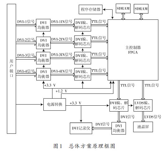
1.1 Overall scheme block diagram
The user inputs 4 DVI signals, and then selects according to the characteristics of the input signals, and displays the video signals on the LCD screen in real time. In addition, the real-time displayed image is returned to the recorder, and the recorder records the current information and the fault information in real time to ensure the correctness of the image display during the full task phase. According to the design requirements, the FPGA chip EP2S30F1020I4 produced by Altera Company is selected as the main control chip, and the configuration chip is selected as EPCS16SI16N. Using the rich logic resources and powerful IP core inside the FPGA, and corresponding external circuits, a flexible, concise and reliable one is constructed. An embedded hardware module for an onboard video graphics processing system. The block diagram of the overall scheme is shown in Figure 1.
1.2 DVI codec design
In many designs, the designer simplifies the circuit for convenience, may not increase the equalizer, and does not process the input signal. Therefore, in the later product testing process, it is easy to have poor signal display quality and poor compatibility, resulting in redesign or rectification of the entire product, delaying product delivery schedule. According to the video characteristics input by the user, this paper uses the equalizer + DVI codec and decoder to convert the input and output signals. This processing has the following advantages: long transmission distance, small signal interference; simple peripheral circuit, flexible and reliable design; fast system speed, flexibility, function scalability, and system compatibility.
In this system, the equalizer DS16EV5110 produced by TI Company is selected, which has the characteristics of low power consumption, small size and simple peripheral circuit. In addition, the DVI codec chip uses TI's chip TFP401 and TFP410, which also has the characteristics of low power consumption, small size, and simple peripheral circuits. The device control pins are directly connected to the FPGA and control the operation of these devices to reduce power consumption. Moreover, the internal logic control of the entire FPGA is simple and reliable.
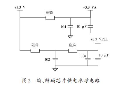
In the hardware circuit design, it is also necessary to consider the influence of high frequency characteristics on the signal. The resolution displayed by the whole system is 1 600×1 200@60 Hz, the signal bit is true color 24 b, the parity is used, the reference clock is 162 MHz, and the DVI coded clock is 10×162 MHz=1.62 GHz. The coding symbol theory The width is only t = 1 1.62 Hz = 0.62 ns, then the maximum change time of the symbol should be within 0.62 4 = 0.16 ns. Considering the reliability and stability of data transmission, the use of dual-pixel transmission can greatly reduce the signal sampling frequency. In addition, the integrity of the PCB layout ground and the power supply decoupling characteristics must be considered. The power supply reference circuit of the codec chip mixed signal is shown in FIG. 2.
Road Traffic Signs are graphical symbols that display traffic regulations and road information. They can make traffic regulations visually, concisely and concisely expressed. At the same time, they also express the content that is difficult to describe in words. They are used to manage traffic and indicate the direction of driving to ensure the smooth flow of roads and the safety of driving. Applicable to highways, urban roads and all special highways, with the nature of the law, vehicles, pedestrians must comply with.
Road Traffic Signs
Road Traffic Signs,Traffic Light Sign,Road Safety Signs,Highway Road Traffic Signs
Yangzhou Heli Photoelectric Co., Ltd. , https://www.heli-eee.com