LED (LighTIng EmitTIng Diode) lighting is light-emitting diode lighting, which is a semiconductor solid light-emitting device. It uses a solid semiconductor chip as a luminescent material, which emits excess energy through carrier recombination in the semiconductor to cause photon emission, and directly emits red, yellow, blue, green, blue, orange, purple, and white light. LED lighting products are lighting appliances manufactured using LEDs as light sources.
1.1 Overview of LEDs 1.1.1 Basic concepts and lighting principles
LEDs are made of III-IV group compounds, such as GaAs (gallium arsenide), GaP (gallium phosphide), GaAsP (gallium arsenide) and other semiconductors, the core of which is the PN junction. Therefore, it has the I-N characteristics of a general PN junction, that is, forward conduction, reverse cutoff, and breakdown characteristics. In addition, under certain conditions, it also has luminescent properties. Under the forward voltage, electrons are injected into the P region from the N region, and holes are injected into the N region from the P region. A part of the minority carriers (minor carriers) that enters the opponent's area recombine with the majority carrier (multiple carriers) and emit light.
Assuming that luminescence occurs in the P region, the injected electrons directly recombine with valence band holes to emit light, or they are first captured by the luminescent center and then recombine with holes to emit light. In addition to this luminescent recombination, some electrons are captured by the non-luminescent center (the center is located near the middle of the conduction band and the dielectric band), and then recombined with the hole. The energy released each time is not large and cannot form visible light. The greater the ratio of the luminescence recombination amount to the non-luminescence recombination amount, the higher the light quantum efficiency. Since the recombination emits light in the minority carrier diffusion region, the light is generated only within the number close to the PN junction surface.
Theory and practice have proved that the peak wavelength of light is related to the forbidden band width Eg of the semiconductor material in the light-emitting region, that is
??? (1.1)
The unit of Eg in the formula is electron volt (ev). If it can produce visible light (wavelength from 380nm purple light to 780nm red light), the Eg of the semiconductor material should be between 3.26 and 1.63ev. Light with a longer wavelength than red light is infrared light. There are now infrared, red, yellow, green and blue light-emitting diodes, but the cost and price of blue diodes are very high, and they are not widely used [2].
1.1.2 Characteristics of LED lighting
1 Limit parameters (1) Allowable power consumption Pm: the maximum value of the product of the forward DC voltage applied to both ends of the LED and the current flowing through it. If this value is exceeded, the LED will become hot or damaged.
(2) Maximum forward DC current IFm: the maximum forward DC current allowed to be added. Exceeding this value can damage the diode.
(3) Maximum reverse voltage VRm: the maximum allowable reverse voltage. Above this value, the light emitting diode may be damaged by breakdown.
(4) Working environment topm: the ambient temperature range where the light emitting diode can work normally. Below or above this temperature range, the LED will not work properly and the efficiency will be greatly reduced.
2 Technical characteristics (1) High luminous efficiency. The luminous efficiency of LED is higher than that of traditional lamps. Most of the power consumption of traditional lamps and lanterns becomes heat loss, and the LED can directly emit colored visible light without filtering, and the power consumption is directly converted into light efficiency, and the luminous efficiency is high.
(2) Low power consumption. The LED adopts direct drive, the response speed is fast, and it can be operated at high frequency. In the case of the same lighting effect, LED power consumption is one-eighth of incandescent lamps and one-half of fluorescent lamps, which is the best choice for power saving and consumption reduction.
(3) Long service life. The LED lamp cap is small in size and light in weight, and is encapsulated in epoxy resin, which can withstand high-strength impact and vibration and is not easily broken. The average service life of LED lamps is longer than traditional lamps.
(4) Strong security. LED has low calorific value, no heat radiation, cold light source, and can be safely contacted; it can accurately control the light type, luminous angle and luminous color; it does not contain mercury, sodium and other substances that may endanger health.
(5) Green and environmental protection. LED is an all-solid luminous body, waste can be recycled, no pollution to the environment, and is conducive to environmental protection.
1.1.3 Comparison of LED and traditional lighting equipment (1) Traditional lighting equipment (1.1) Incandescent lamp: Incandescent lamp is the oldest lamp with extremely wide application. Its luminescence principle is based on the passage of filament in vacuum or neutral gas The phenomenon of heat radiation caused by current heating to incandescent state. Its advantages are simple structure, low price, convenient use, and good color rendering; the disadvantages are high heat generation, low luminous efficiency, short service life, and special attention should be paid. If the power supply voltage is increased by 5, the lamp life will be shortened by 50% .
(1.2) Fluorescent lamps: The family of fluorescent lamps includes ordinary fluorescent lamps and compact fluorescent lamps. Its principle is to use mercury vapor to generate an arc discharge under the action of an applied voltage, which emits a little visible light and a large amount of ultraviolet light. The ultraviolet light also stimulates the fluorescent powder coated on the inner wall of the lamp tube to make it emit a large amount of visible light. Compact fluorescent lamps can gradually replace incandescent lamps: their power saving rate is high, and the brightness of 15W compact fluorescent lamps is comparable to that of 75W incandescent lamps. Long lifespan, with an average lifespan of 8000 hours, up to 20,000 hours, and incandescent lamps only 1,000 hours to 2000 hours.
(1.3) Discharge lamp: The gas sealed in the bulb glows through the discharge of two electrodes. All such lamps need to be equipped with a ballast to limit the arc.
(2) New-type lighting equipment LED
LED (Lighty EmitTIng Diode), also known as light-emitting diode, it uses a solid semiconductor chip as a light-emitting material, the terminal voltage of the PN junction constitutes a certain barrier, the barrier decreases when a forward bias voltage is applied, and most of the P and N regions Carriers diffuse to each other. Since the electron mobility is much greater than the hole mobility, a large number of electrons will diffuse into the P region, which constitutes the injection of minority carriers in the P region. These electrons recombine with holes in the valence band, and the energy obtained during recombination is released in the form of light energy. This is the principle of PN junction luminescence [7]-[11].
1.1.4 LED lamps have high luminous efficiency, almost all the spectrum is focused on visible light, and the frequency efficiency can reach 80% -90%, and the monochromaticity of the light is good. The spectrum is narrow, and colored visible light can be directly emitted without filtering.
Table 1-1 Comparison of luminous efficiency
| Types of lamps | Light effect / (Lumen / Watt) |
| Incandescent lamp | 5-10 |
| Tungsten halogen lamp | 5-10 |
| Fluorescent lamp | 40-80 |
| sodium lamp | 40-110 |
| LED lights | 60-250 |
Table 2-2 Comparison of power consumption of street lamps
| Daily lighting hours | Annual electricity (kwh / year) | Unit price of electricity (yuan / kwh) | Annual electricity fee / yuan | 3 years electricity fee / yuan | |
| HPS | 10 | 54750 | 0.8 | 43800 | 131400 |
| LED lighting | 10 | 21900 | 0.8 | 17520 | 52560 |
1.2 Overview of the sound and light control circuit The sound control delay switch is a kind of no contact point. The sound effect is used to stimulate the pickup to perform the sound-electricity conversion under specific ambient light to control the opening of the electrical appliance. Energy-saving electronic switch [12].
Features and functions:
(1) Sound start control: by making certain sounds by hand (or whistling, shouting, etc.) near the switch, the lights and electrical appliances can be turned on immediately, handy.
(2) Automatic metering: using photosensitive control, the switch will not turn on the electrical appliances due to sound during the day or when the light is strong.
(3) Delayed self-closing: Once the switch is controlled to open, it will be automatically shut off after a delay of tens of seconds, reducing unnecessary waste of electrical energy and being practical and convenient.
(4) The service life of delayed electrical appliances.
(5) Wide range of uses: This product can be used for automatic delay lighting in various corridors, corridors, bathrooms, balconies, basement garages and other places.
2 Scheme demonstration
2.1 Power control
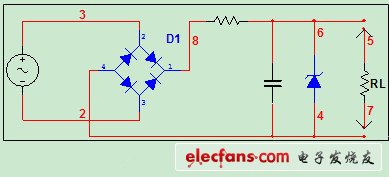
Figure 2-1 Rectifier voltage regulator circuit diagram
First of all, in the above picture, we can see that the 220V we use every day is added between the unidirectional bridge rectifier circuit composed of 4 diodes. After the 220V AC is rectified, it is sent to the R resistor, and the current is limited through the R circuit. Carry out filtering and voltage stabilizing tube to stabilize the voltage, so as to obtain a stable voltage of DC to maintain the normal work of the circuit thereafter.
(1) Rectification:
For the four diodes, from left to right and from top to bottom, we divide them into VD1, VD2, VD3, and VD4. When the positive half cycle of the AC signal, the diodes VD2, VD3 conduct, VD1, VD4 cut off; when the signal changes to the negative half cycle, VD1, VD4 conduct, VD2, VD3 cut off. Both the positive and negative half cycles have current flowing through the back load resistor, and the current direction flowing through the back load resistor is the same in both the positive half cycle and the negative half cycle, so that the DC component of the output voltage is improved and the pulse component is reduced .
(2) Filtering:
No matter what kind of rectifier circuit, their output voltage contains a large ripple component. Except that it can be directly used as the power supply of the amplifier in some special occasions, certain measures are usually taken. On the one hand, the pulsating part of the output voltage is reduced as much as possible, and the DC component in the other part is kept as much as possible to make the output voltage close to Ideal DC voltage. Such a measure is filtering.
After the capacitors are connected in parallel, in the positive half of the signal, when the diodes VD2 and VD3 conduct, when the diode conducts, in addition to a current flowing to the load, there is also a current charging the capacitor. The polarity of the capacitor voltage is up and down. If the internal resistance of the diode is ignored, the output voltage is equal to the input voltage when the diode is turned on. When the signal reaches the maximum value, it begins to drop, and the voltage on the capacitor will gradually drop due to discharge. When the signal is less than the capacitor voltage, the diodes VD2 and VD3 are reverse biased and thus non-conductive, so the capacitor voltage decreases exponentially with a certain time constant until the next half cycle, when the absolute value of the signal is greater than the capacitor voltage, Diodes VD1 and VD4 are turned on.
The following conclusions can be obtained for capacitor filtering:
â‘ After the capacitor filter is added, the DC component of the output voltage increases.
â‘¡After the capacitor filter is added, the ripple component in the output voltage is reduced. This is due to the energy storage effect of the capacitor. When the diode is conducting, the capacitor is charged, storing energy, and then gradually discharging, transferring the energy to the load, so the output waveform is relatively smooth.
â‘¢ The larger the time constant of capacitor discharge Ï„ = RC, the slower the discharge process, the higher the output voltage, and the less the pulsation component, that is, the better the filtering effect.
④ After connecting the capacitor, the conduction time of the rectifier diode is shortened. The conduction angle of the diode is <180 °, and the larger the capacitor discharge time constant, the smaller the conduction angle. After the capacitor filter is added, the average output current is higher than the original, but the conduction angle is reduced. Therefore, a large rush current flowing through the rectifier in a short conduction time is detrimental to the life of the tube, so it must be selected. Larger capacity rectifier diode.
(3) Voltage stabilization:
The voltage stabilizing principle of the voltage stabilizing diode: the characteristic of the voltage stabilizing diode is that after breakdown, the voltage across the two ends remains basically unchanged. In this way, when the voltage regulator is connected to the circuit, if the voltage of each point in the circuit fluctuates due to fluctuations in the power supply voltage or other reasons, the voltage across the load will remain basically unchanged.
2.2 LED drive part 2.2.1 Constant current and constant voltage At present, low-power LED products widely use two drive circuit forms, namely constant current drive and constant voltage drive. The current output by the former circuit is constant, and the output voltage changes with the change of the load; the latter output voltage is fixed, and the output current changes with the increase and decrease of the load (number of LEDs).
(1) Constant current drive circuit Under the constant current drive working mode, there are two other drive working modes. One is a constant voltage source for multiple constant current sources, and each constant current source supplies power to each LED separately. The combination of this method is flexible, all the way LED failure, does not affect the work of other LEDs, but the cost will be slightly higher. The other is that LEDs powered directly by a constant current source operate in series or in parallel. Its advantage is that the cost is a bit lower, but the flexibility is poor, and it is necessary to solve the problem of a certain LED and not affect the operation of other LEDs. The multi-channel constant current output power supply of LED will be better in terms of cost and performance. The constant current drive of LED has the following characteristics.
â‘ It is ideal to use constant current drive circuit to drive LED, the disadvantage is that the price is higher;
â‘¡Although the constant current drive circuit is not afraid of short circuit of the load, it is strictly forbidden to completely open the load;
â‘¢ The output current of the constant current drive circuit is constant, but the output DC voltage varies within a certain range with the size of the LED load;
â‘£To limit the number of LEDs used, because it has the problem of maximum withstand current and voltage value.
(2) Constant voltage drive circuit â‘ After determining the parameters of the constant voltage circuit, the constant voltage circuit outputs a fixed DC voltage, and the output DC current changes with the change of the LED load;
â‘¡ Although the constant voltage circuit is not afraid of open load, it is strictly forbidden to completely short-circuit the load;
â‘¢The voltage change of the rectified output will affect the LED brightness;
â‘£To make each string connected in parallel and drive a constant voltage circuit to drive LED strings with even brightness, appropriate resistance needs to be added.
2.2.2 Conventional bucks are divided by application. The LED driver IC market has three major categories, namely consumer electronics, automotive lighting, architectural decoration and household lighting. The application characteristics of consumer electronics products are battery-based energy, the voltage is generally 4.2 ~ 8.4V, so low-voltage, low-current LED drivers best meet the needs, and is a product with large application and wide application. In terms of automotive lighting products, since the power supply comes from the car battery, which is generally 48V, a higher voltage step-down LED driver IC is required. As for architectural decoration lighting and home lighting, you need to directly convert AC power to DC power LED driver IC, that is, convert AC to DC power, and at the same time complete the matching with the LED voltage and current. Therefore, LED driver ICs in different applications will also be different. In the home lighting circuit, there are several ways to obtain constant voltage:
(1) Voltage reduction of conventional transformers The disadvantages of this type of power supply are heavy weight and large volume. The working efficiency of the power supply is very low, generally 45% to 60%. Because the reliability of the work is not high, it is generally rarely used.
(2) Step-down of electronic transformer The shortcoming of this power supply structure is low conversion efficiency, narrow voltage range, generally 180 ~ 240V, and large ripple interference.
(3) Capacitor step-down The LED driving power supply is easily affected by the voltage fluctuation of the power grid, and the working efficiency of the power supply is low. At this time, due to the charging and discharging of the capacitor, the instantaneous current through the LED is very large, which is easy to damage the LED drive control chip. Of course, such protection can be avoided with proper protection.
(4) Resistance step-down This power supply has low working efficiency and low reliability. Because the circuit is stepped down through the resistor, it is greatly disturbed by the change of the grid voltage, and the working current of the LED is greatly affected by the change of the grid voltage. And the buck resistor itself consumes a large part of the power.
(5) RC step-down switching power supply The advantages of this type of LED drive power supply are that the voltage regulation range is relatively wide and the power supply operating efficiency is relatively high, generally 70% to 80%, and the application is wide. The disadvantages are that the switching frequency is not easy to control, the load voltage ripple coefficient is large, and the load adaptability is abnormal in abnormal situations.
(6) PWM-controlled switching power supply As far as the current is concerned, the PWM-controlled LED drive power supply is ideal, because the output voltage or current of this switching power supply is very stable. The power conversion work efficiency is high, generally up to 80% to 90%, and the output voltage and output current are very stable. This mode of LED drive power is mainly composed of four parts. They are: main input rectification and filtering part, output rectification and filtering part, PWM voltage stabilizing control part, and switching transformation part. But it is also the most expensive and technically complex LED current control solution. They are different from linear regulators and simple resistor current stabilization schemes, and are susceptible to electromagnetic interference (EMI), which presents designers with another challenge to overcome. For medium to high power solutions, or applications that need to handle a wide input voltage range, switching regulators are the only viable option [4] [5].
2.2.3 Isolated and non-isolated According to the power input and output circuit form, it can also be divided into isolated drive and non-isolated drive. The former is represented by switching power supply, while the latter mainly includes capacitor buck and constant current / constant voltage IC. The related performance, power consumption, cost and main applications are shown in Table 2-1.
Table 2-1 Comparison of low-power LED driving schemes
| kind | performance | Power consumption and cost | main application | |
| Isolated drive | Electric pump switching power supply | Input and output isolation, safe and stable, no electromagnetic interference, large output current, but relatively low voltage | Moderate power consumption, need to control Ic, higher cost | Suitable for a small number of high-power LED applications |
| Inductive switching power supply | Input and output isolation, safe and stable, small size, high efficiency, multiple output, good control performance, dimmable, constant voltage, constant current, but there is electromagnetic interference | Large power consumption and high cost | Application of high power or current in hundreds of milliamperes | |
| Non-isolated drive | Capacitor buck | Input and output are not isolated, there are hidden dangers, low efficiency, no electromagnetic interference, constant current drive, LED brightness is consistent, but not suitable for load changes | Low power consumption and low cost | Suitable for low power or low current applications |
| Constant current / constant voltage Ic | The input and output are not isolated, there are hidden dangers, the efficiency is higher than that of the capacitor step-down type, and it can be constant voltage and constant current without electromagnetic interference | Low power consumption and moderate cost | The number of connected LEDs is small, low-power LED applications |
Since the LED is a device whose current changes significantly with voltage, when the LED is turned on, a small change in its forward voltage can cause a huge change in the LED current. For the regulated LED drive power supply, when the load changes, the current fluctuation is large, and the LED will be damaged when working at a large current for a long time. Experiments show that when the actual current flowing through the LED is 70% of the maximum allowable current, the LED's luminous efficacy is optimal. At the same time, because the voltage temperature coefficient of the PN junction of the light emitting diode is about -2mV / ℃, when the temperature of the LED is poor, the operating current will also change significantly from the initial stage, which is also the rapid aging of various LED products on the market. The main reason. Obviously, ensuring the stability of the LED drive current is particularly important for the LED's anti-aging. Therefore, the constant current driving power supply is an ideal LED driving method. Usually, LEDs are driven by dedicated constant current sources or driver chips. When limited by volume and cost, the most economical and practical method is to use a capacitive step-down power supply. Using it to drive low-power LEDs has the advantages of not being afraid of load short circuits and simple circuits, and a circuit can drive 1 to 70 low-power LEDs. However, this current surge when the power circuit starts, especially frequent start-ups, will cause damage to the LED. Of course, such protection can be avoided with proper protection.
The typical circuit of a capacitive step-down power supply is shown in the figure below. C1 is a step-down capacitor (using a metalized polypropylene capacitor), and R1 provides a discharge circuit for C1. Capacitor C1 provides a constant operating current for the entire circuit. Capacitor C2 is an electrolytic capacitor, and its withstand voltage depends on the number of LEDs connected in series (about 1.5 times or more than its total voltage). Its main function is to suppress the voltage mutation caused by the instant of power-on, thereby reducing the voltage impact on the LED. The impact of life. R4 is the bleeder resistor of capacitor C2, and its resistance value should increase appropriately with the increase of the number of LEDs.
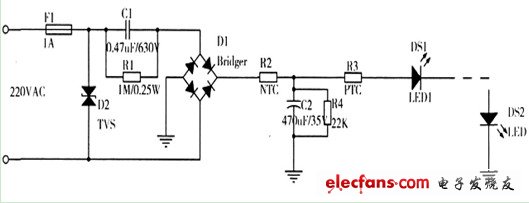
Figure 2-2 Typical circuit diagram of a capacitor step-down power supply
It should be noted that the appropriate capacitance must be selected according to the current size of the load, rather than the voltage and power of the load. The relationship between the capacity C of the buck capacitor C1 and the load current Io can be approximated as: C = 14.5I, where C The unit of capacity is μF, and the unit of Io is A. The current-limiting capacitor must be a non-polar capacitor, and the withstand voltage of the capacitor must be above 630V.
2.2.4 Protection circuit Because the capacitor step-down power supply is a non-isolated power supply, a large current will be generated at the moment of power-on, which is called the inrush current. In addition, due to the influence of the external environment such as the induction of lightning strikes, various surge signals will be invaded from the power grid system, and some surges will cause damage to the LED. The LED's anti-surge current and anti-reverse voltage capabilities are compared, it is also very important to strengthen the protection in this area, especially some LED lights are installed outdoors, such as LED street lights. Therefore, the LED drive power must have the ability to suppress the intrusion of the surge and protect the LED from being damaged. This circuit uses NTC (negative temperature coefficient thermistor) to limit the sudden change of current, and uses PTC (positive temperature coefficient thermistor) to automatically adjust the current size so that it tends to a certain change range, and at the same time at the power input end TVS (Transient Voltage Suppressor) to avoid voltage overload.
(1) NTC protection
NTC is the abbreviation of NegaTIve Temperature Coefficient, which means negative temperature coefficient. It generally refers to semiconductor materials or components with a large negative temperature coefficient. The so-called NTC thermistor is a negative temperature coefficient thermistor. The simplest and most effective way to limit the inrush current is to connect an NTC thermistor in series with the line input, as shown in Figure 2-2 R2. Since NTC thermistors exhibit high impedance during cold start, the inrush current is limited. When the thermal effect of the current increases the temperature of the NTC thermistor and the resistance of the NTC drops sharply, the current limiting effect on the system will be small. Because the impedance of the NTC thermistor in the thermal state is not zero, it will cause power loss, of course, this loss is very small [6].
(2) PTC protection
PTC (Positive Temperature CoefflCient) refers to a thermistor phenomenon or material that has a sharp increase in resistance at a certain temperature and a positive temperature coefficient. In order to make the current in the circuit tend to stabilize under normal operation, this circuit also uses a PTC thermistor, such as R3 in Figure 1. After the current passes through the PTC thermistor, the temperature rises, that is, the temperature of the heating element rises. When the temperature exceeds the Curie point, the resistance increases, thereby limiting the current increase, so the current drop causes the component temperature to decrease, and the resistance value decreases. The circuit current is increased, the temperature of the component is increased, and the cycle is repeated, so it has the function of keeping the temperature within a specific range.
The PTC element is connected in series in the circuit. Under normal circumstances, it is in a low-impedance state to ensure the normal operation of the circuit. When the circuit is short-circuited or enters an abnormally large current, the self-heating of the PTC element causes its impedance to increase and limit the current to a small enough Play the role of overcurrent protection. When the overcurrent fault is eliminated, the PTC element automatically recovers to the low resistance state. It not only avoids maintenance and replacement, but also avoids the continuous cycle of open and closed states that may cause circuit damage [16].
(3) TVS protection Transient Voltage Suppressor (Transient Voltage Suppressor), referred to as TVS, is an efficient protection device developed on the basis of the voltage regulator tube, which is mainly used for fast overvoltage protection of circuit components. When the two poles of the TVS tube are impacted by reverse transient high energy, it can change the high impedance between the two poles to a very low impedance at a speed of the order of 10 to 12 seconds, absorb the high energy surge, and change the voltage between the two poles. The clamp is located at a predetermined value to protect the components in the electronic circuit from various surge pulses.
For overvoltage protection, this circuit is to connect TVS in parallel to the power input, as shown in Figure 2-2, D2, so that the voltage can be maintained within the maximum TVS tolerance, when the voltage is higher than the TVS breakdown point When the overvoltage phenomenon occurs, current can flow through the TVS, thereby protecting LED lighting fixtures.
Experiments show that after the pointer multimeter is connected into the circuit, the phenomenon that the pointer suddenly deflects at a large angle is greatly improved at the moment of circuit energization, and the impact of surge current on the LED is effectively prevented. At the same time, after starting for a period of time, the current has dropped and gradually stabilized. Replacing NTC with 1W metal film resistor or wire-wound resistor can also meet the requirements. TVS or varistor can be used for overvoltage protection [14] [15].
2.3 Sound and light control part
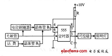
Figure 2-3 Acousto-optic control circuit block diagram
2.3.1 555 timer
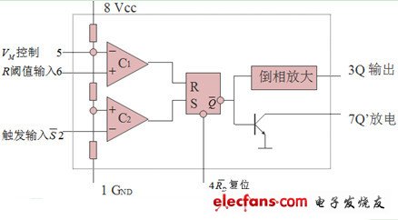
Figure 2-4 Internal block diagram of 555 timer
The 555 timer is a medium-sized integrated device that combines analog and digital functions. Generally produced by the bipolar process is called 555, and produced by the CMOS process is called 7555. In addition to the single timer, there are corresponding dual timers 556/7556. The power supply voltage range of the 555 timer is wide, which can be 4.5 V ~ 16V work, 7555 can work in 3 ~ 18V, output drive current is about 200mA, so its output can be compatible with TTL, CMOS or analog circuit level.
The 555 timer has low cost and reliable performance. It only needs a few external resistors and capacitors to realize pulse generation and conversion circuits such as multivibrator, monostable trigger and Schmitt trigger. It is also widely used as a timer in instrumentation, household appliances, electronic measurement and automatic control. The internal circuit block diagram and external pin arrangement diagram of the 555 timer are as shown in the figure. It includes two voltage comparators, three equivalent series resistors, an RS trigger, a discharge tube T and power output stage. It provides two reference voltages VCC / 3 and 2VCC / 3.
The function of the 555 timer is mainly determined by two comparators. The output voltages of the two comparators control the state of the RS trigger and the discharge tube. Add a voltage between the power supply and ground. When pin 5 is left floating, the voltage at the non-inverting input of voltage comparator C1 is 2VCC / 3, and the voltage at the inverting input of C2 is VCC / 3. If the voltage at the trigger input terminal TR is less than VCC / 3, the output of the comparator C2 is 0, and the RS flip-flop can be set to 1, so that the output terminal OUT = 1. If the voltage at the threshold input terminal TH is greater than 2VCC / 3, and the voltage at the TR terminal is greater than VCC / 3, the output of C1 is 0 and the output of C2 is 1. The RS flip-flop can be set to 0 to make the output at level 0.
The medium-scale integrated circuit developed by American Signetics Company in 1972 to replace the mechanical timer got its name because of the design of three 5kΩ resistors at the input end. This circuit became popular all over the world. Currently, there are four popular products: two BJTs: 555, 556 (including two 555); two CMOS: 7555, 7556 (including two 7555).
The 555 timer can be said to be a model of combination of analog circuits and digital circuits.
Each of the two comparators C1 and C2 has an input connected to a voltage divider composed of three resistors R, and the output of the comparator is connected to an RS flip-flop. In addition there are output stage and discharge tube. The drive current of the output stage can reach 200mA.
The reference voltages of the comparators C1 and C2 are UA and UB respectively, and the output state of the RS flip-flop can be judged according to the other input terminals of C1 and C2-the trigger input and the threshold input. When the reset terminal is low, the RS flip-flop is forced to reset. If no reset operation is required, the reset terminal should be connected to high level.
Application of 555 timer:
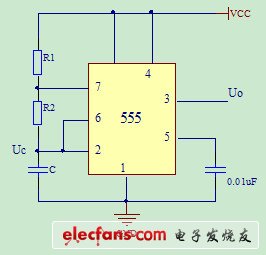
Figure 2-5 Typical application circuit diagram of 555 timer
(1) Form Schmitt trigger, used for TTL system interface, shaping circuit or pulse amplitude detection, etc .;
(2) Form a multivibrator and form a signal generating circuit; as shown above, the oscillation period:
(2.1)
(3) Form a monostable trigger, used for timing delay shaping and some timing switches.
The 555 application circuit can be combined with one or more of these three methods to form various practical electronic circuits, such as timers, frequency dividers, pulse signal generators, component parameters and circuit detection circuits, toy game machine circuits , Audio alarm circuit, power exchange circuit, frequency conversion circuit, automatic control circuit, etc. [13].
2.3.2 Control of unidirectional thyristor Before analyzing its working principle, let me introduce the working principle of unidirectional thyristor.
The thyristor is a P1N1P2N2 four-layer three-terminal structure element with a total of three PN junctions. When analyzing the principle, it can be regarded as composed of a PNP tube and an NPN tube. When the anode A is added with a forward voltage, BG1 and The BG2 tubes are in an enlarged state. At this time, if a positive trigger signal is input from the control electrode G, a base current Ib2 flows through BG2, and after being amplified by BG2, its collector current Ic2 = β2Ib2. Because the collector of BG2 is directly connected to the base of BG1, Ib1 = Ic2. At this time, the current Ic2 is amplified by BG1 again, so the collector current Ic1 of BG1 = β1Ib1 = β1β2Ib2. This current flows back to the base of BG2, which represents positive feedback, causing Ib2 to continue to increase. As a result of such a positive feed cycle, the current of the two tubes increases sharply, and the thyristor makes saturation conduct. Due to the positive feedback function formed by BG1 and BG2, once the thyristor is turned on, even if the current of the control electrode G disappears, the thyristor can still maintain the on state. Since the trigger signal only acts as a trigger, there is no shutdown Function, so this thyristor is irreversible.
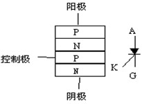
Figure 2-6 Unidirectional SCR
Since the SCR only has two working states of on and off, it has switching characteristics. This characteristic requires certain conditions to be converted. For specific conversion conditions, see Table 2-2. Table of thyristor on and off conditions. Shown: Table 2-2 SCR turn-on and turn-off conditions table
| status | condition | Explanation |
| From off to on | 1. The anode potential is higher than the cathode potential 2. The control pole has enough forward voltage and current | Both are indispensable |
| Keep on | 1. The anode potential is higher than the cathode potential 2. The anode current is greater than the sustain current | Both are indispensable |
| From on to off | 1. The anode potential is lower than the cathode potential 2. The anode current is less than the maintenance current | Any condition |
2.3.4 Voice control part When the sound of sufficient signal comes in, the voice control part converts the voice signal into an electric signal, and amplifies its signal through the transistor B1, so that the size of the signal can trigger the transistor B2. The first and second stages of the circuit are connected by resistors and capacitors, so they are called resistance-capacitive coupling amplifier circuits. The advantage of resistance-capacitance coupling is that because the front and rear stages are connected by capacitors, the DC circuits of each stage are not connected to each other, and the static operating points of each stage are independent of each other, so as not to affect each other. Design and debugging bring great convenience. Moreover, as long as the coupling capacitor is selected large enough, the output signal of the previous stage can be added to the input terminal of the next stage with little attenuation within a certain frequency range, so that the signal is fully utilized.
When the sound signal disappears, the diode is cut off, and the triode is no longer working, but the capacitor is discharged, so that the triode can still be turned on for a period of time, and can also provide current to the unidirectional thyristor. Such a delay does not cause the lamp to turn off when the signal disappears, and the practicability is high. After the capacitor is discharged, the circuit resumes when there is no signal at the beginning. When the sound signal comes in again, repeat the above situation.
3 Design process discussion
3.1 Circuit composition
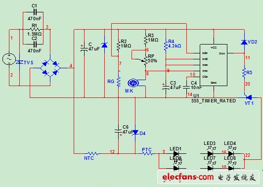
Figure 3-1 LED driver circuit diagram
The LED drive circuit is shown in Figure 3-1. It can be divided into two parts: main circuit and control circuit. The main circuit is a series circuit of LED load and unidirectional thyristor VT1. The control circuit can be divided into two parts: DC power supply and photo-acoustic controlled monostable trigger. The DC power supply is composed of a half-wave rectifier circuit, a capacitor filter circuit, and a transistor series voltage stabilizing circuit. The photoacoustic controlled monostable trigger consists of a photoelectric conversion circuit composed of a resistor R2 and a photoresistor RG, an acoustoelectric conversion circuit composed of a resistor R3, a potentiometer RP and an electret microphone MK, and a CMOS 7555 timer Monostable trigger.
3.2 Working principle When the light is strong during the day, the photoelectric conversion circuit outputs a low level, sending the R terminal of the 7555 timer, forcing the monostable trigger to output a low level, so that the VT1 is in the off state, thereby ensuring the light bulb when the light is strong during the day not bright. When the light is weak at night, the photoelectric conversion circuit outputs a high level to the R terminal of the 7555 timer, which does not affect the output state of the monostable trigger. At this time, a sufficiently strong sound electrical signal generated by the sound-electricity conversion circuit can pass through the TR terminal of the 7555 timer to make the monostable flip-flop flip from the steady-state low-level output to the transient high-level output, so that VT1 Turn on and light the lamp. Adjust the RP in the acoustoelectric conversion circuit to adjust the sensitivity of voice control. The duration TL of the light is the transient time of the monostable trigger, which is determined by the resistor R3 and the capacitor C3.
The diode VD2 in the picture is used to prevent the bulb from extinguishing prematurely. If there is no VD2, when the light is weak at night and the light bulb is turned on under sound control, the bright light shines on RG. As in the case of daytime light intensity, the photoelectric conversion circuit outputs a low level to send the R terminal of 7555 timer , Forcing the monostable trigger to output a low level, so that VT1 is turned off when the current crosses zero, so that the bulb does not reach the time determined by R3 and C3 and extinguishes in advance. With VD2, the output of the photoelectric conversion circuit can be locked at a high state during the high level of the monostable flip-flop, thereby ensuring that the duration of the light is determined by R3 and C3.
3.3 Parameter design The parameter design principle of the lighting photoacoustic control circuit is to reduce power consumption as much as possible on the premise of achieving its control kinetic energy and reducing costs. The monostable trigger in the circuit uses the CMOC 7555 timer instead of the TTL 555 timer, the purpose of which is to reduce power consumption. Only the design points of some main parameters of each part of the circuit are discussed below.
3.3.1 Parameter design of the main circuit The parameter design of the main circuit is very simple, just determine the voltage level of the AC voltage UAC and select the specific model of the thyristor VT1 according to the rated voltage and rated current of the controlled bulb. When choosing the thyristor model, the bidirectional thyristor with a smaller trigger voltage and trigger current should be selected as much as possible, so that the resistance of the current limiting resistor R5 can be appropriately increased to reduce the dynamic power consumption of the monostable trigger.
3.3.2 Parameter design When designing the parameters of this part of the circuit, first determine its operating voltage. The working voltage range of CMOS 7555 timer is 3 ~ 18V. Considering that the trigger voltage of most thyristors is generally between 2 ~ 5V, the typical working voltage of electret microphone is usually 4 ~ 5V, so the working voltage can be about 5V .
Selection of buck capacitor value:
For the current I0 of 20mA consumed by the load, the value of the buck capacitor needs to be at least 0.29μF. Due to the increase of the high-voltage zener diode in the figure, the diode also needs to consume a large current during operation. In addition, to ensure the reliable operation of the capacitor C, The withstand voltage selection should be greater than 2 times the power supply voltage, so two 0.47uF / 630V capacitors should be selected to work in parallel.
Rectifier and filter circuit:
The maximum voltage of a single diode on the rectifier bridge (the effective value of the input voltage) = 318.4V, so the commonly used rectifier diode 1N4007 (URM = 1000V, IF = 1A) is used.
为使输出端得到平滑的负载电压,一般å–RLC≥(3~5)T/2,其ä¸RL为负载阻抗,T为输入信å·å‘¨æœŸ(0.02s),å¯å¾—C≥24.38μF。原则上,电容值å–的越大,输出电压越平滑,其纹波值越å°ã€‚但是éšç€ç”µå®¹å®¹é‡çš„增大,一般其体积也éšä¹‹å¢žå¤§ï¼Œè€ƒè™‘到该电路æ¿é¢ç§¯ï¼Œå®žå–47μF/160V的电解电容。
工作电压确定åŽï¼Œè¦ç‰¹åˆ«è€ƒè™‘åˆ°ä»¥ä¸‹å‡ ç‚¹ã€‚
(1)光电转æ¢ç”µè·¯ä¸çš„RG应尽å¯èƒ½é€‰æ‹©æš—电阻较大的光æ•ç”µé˜»ã€‚对于用于路ç¯æŽ§åˆ¶çš„照明光声控制电路一般å¯ä½¿çŽ¯å¢ƒå…‰çº¿åœ¨10XLå·¦å³,å³å¯é€šè¿‡,声音控制使ç¯æ³¡ç‚¹äº®ã€‚而CMOSåž‹7555定时器R端的转æ¢ç”µåŽ‹ä¸ºVDD/2,故光电转æ¢ç”µè·¯å‚æ•°å¯æŒ‰ä¸‹å¼è®¾è®¡: 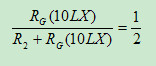 (3.1)
(3.1)
å¼ä¸ä¸ºå…‰çº¿åœ¨10XL时光æ•ç”µé˜»RG的阻值。故应尽å¯èƒ½é€‰æ‹©è¾ƒå¤§çš„å…‰æ•ç”µé˜»,å› ä¸ºè¾ƒå¤§,按å¼(3.1)算得的也较大,从而å¯å‡å°å…‰ç”µè½¬æ¢ç”µè·¯çš„é™æ€ç”µæµå’ŒåŠŸè€—。
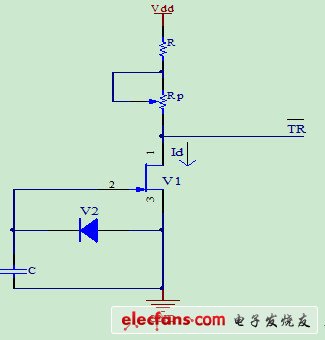
图3-2声电转æ¢éƒ¨åˆ†
(2)声电转æ¢ç”µè·¯ä¸çš„MK应尽å¯èƒ½é€‰æ‹©å·¥ä½œç”µæµIMK较å°çš„é©»æžä½“è¯ç’。上图为包括驻æžä½“è¯ç’内部电路的声电转æ¢ç”µè·¯ã€‚由图å¯çŸ¥,é©»æžä½“è¯ç’的工作电æµå°±æ˜¯é©»æžä½“è¯ç’内部场效应管的é™æ€æ¼æžç”µæµã€‚å› æ¤,IMK越å°,声电转æ¢ç”µè·¯çš„é™æ€åŠŸè€—就越å°ã€‚
(3)定时元件R4的阻值å–值è¦é€‚当。ç¯äº®çš„æŒç»æ—¶é—´TL(å³å•ç¨³æ€è§¦å‘器的暂æ€æ—¶é—´)为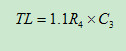 (3.2)
(3.2)
通常,å–TL=30~50s。显然,R4的阻值å–得越大,C3的电容é‡å°±å¯å–得越å°,这有利于å‡å°ä½“积和é™ä½Žæˆæœ¬ã€‚åŒæ—¶ï¼ŒR2的阻值å–得大一些,还å¯å‡å°å…¶åŠŸè€—。但考虑到7555定时器内部è¿ç®—放大器两个输入端电阻的平衡,R4的阻值ä¸èƒ½å–得太大,一般å¯å–1MΩ左å³ã€‚TLå’ŒR4çš„å‚数确定åŽï¼Œå³å¯ç”±å¼(3.2)求得C3的电容é‡ã€‚è‹¥R4å–1M,则C3å–47uFå¯å»¶è¿Ÿ50så·¦å³ã€‚
4 结论按照电路图完æˆçš„电路设计,在光照下有声å“LEDç¯ä¸äº®ï¼Œåœ¨é»‘暗环境下,有声å“LEDç¯äº®ï¼Œå¹¶å»¶æ—¶50s。在电路图ä¸ï¼Œå…±æŽ¥å…¥äº†28åªLED,å¯ä»¥è¾¾åˆ°çš„功率为了2Wå·¦å³ï¼Œå¯ä»£æ›¿æ™®é€šçš„20W的白炽ç¯ï¼Œå®Œå…¨ç¬¦åˆå°åŠŸçŽ‡LED照明需è¦ã€‚通过本次实验设计,了解了常用的é™åŽ‹çš„方法,熟悉了使用555定时器设计声控开关,并掌æ¡äº†å°åŠŸçŽ‡LED的驱动。
You will find various programming tools such as channel sliders , scene buttons and an led display on our Dmx Console . The DMX Console is main one of dj lighting equipment . Our this DMX console have 192 DMX channels, 12 scanners of 16 channels each, 30 banks of 8 programmable scenes, 6 programmable chases of 240 scenes, 8 sliders for manual control of channels. Our auto mode program can control speed. The DMX console is an affordable solution for controlling DMX products and the stage lighting.
DMX Console
Dmx Console,Portable Dmx Console,Dmx Lighting Console,Oem Stage Light Dmx Console
Shenzhen Iseeled Technology Co., Ltd. , https://www.iseeledlight.com