UFO-shaped LED floor lamp
Summary
This work is based on FPGA ADC0809 acquisition control circuit. ADC0809 is a CMOS process 8-channel, 8-bit successive approximation A/D analog-to-digital converter manufactured by National Semiconductor. It has an 8-channel multiplexer inside, which can latch the decoded signal according to the address code and only strobe one of the 8 analog input signals for A/D conversion.
Abstract
ADC0809 is produced naTIonal semiconductor CMOS 8 channel, eight successive approximaTIon A/D analog-to-digital converter. Its internal have A 8 channel mulTIplex switch, it can according to the address latch signal After decoding, only gate 8 analog input signals of an A/D conversion.
Design task
FPGA-based ADC0809 control circuit design, and clarify its control principle.
2. Introduction to ADC0809
2.1. Main features of ADC0809
18 8-bit A/D converters with a resolution of 8 bits.
2 has a conversion start and stop control terminal.
3 conversion time is 100μs
4 single +5V power supply
5 analog input voltage range 0 ~ +5V, no zero and full scale calibration.
6 working temperature range is -40 ~ +85 degrees Celsius
7 low power consumption, about 15mW
2.2. ADC0809 external characteristics (pin function)
The 1ADC0809 chip has 28 pins. The function of each pin is explained below.
2IN0~IN7: 8 analog inputs.
3D0~D7: 8-bit digital output.
4ADDA, ADDB, ADDC: 3-bit address input line for strobing one of the eight analog inputs
5ALE: Address latch enable signal, input, active high.
6START: A/D conversion start signal, input, active high.
7EOC: A/D conversion end signal, output, when the A/D conversion ends, this terminal outputs a high level (the low period during the conversion period).
8OE: Data output enable signal, input, active high. When the A/D conversion ends, a high level is input to this terminal to open the output tristate gate and output the digital quantity.
9CLK: Clock pulse input. The clock frequency is required to be no higher than 640KHZ.
10REF(+), REF(-): Reference voltage.
11Vcc: Power supply, single +5V.
12GND: Ground.
2.3. How ADC0809 works
First enter the 3-bit address and let ALE=1, store the address in the address latch. This address is decoded to strobe one of the eight analog inputs to the comparator. The START rising edge will reset the register successively. The falling edge initiates an A/D conversion, after which the EOC output signal goes low, indicating that the conversion is in progress. Until the A/D conversion is completed, EOC goes high, indicating that the A/D conversion is complete, and the result data has been stored in the latch. This signal can be used as an interrupt request. When the OE input is high, the output tri-state gate is opened and the digital result of the conversion is output to the data bus.
3. Theoretical analysis and calculation
3.1. System design principle
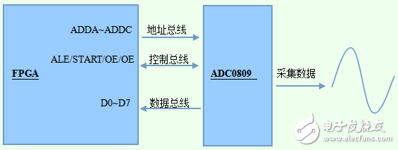
Figure 3-1: System Design Schematic
Working principle: The FPGA inputs the acquisition port address through the control bus. This address is decoded by ADC0809 and strobed one of the 8-channel analog acquisition input ports. The FPGA output control signal causes the START pin signal of AD to be high, the rising edge will successively approach the register reset, and the falling edge initiates the A/D conversion. The ADC0809's EOC pin output signal goes low after the conversion is initiated, indicating that the FPGA AD conversion is in progress. Until the A/D conversion is completed, the EOC pin goes high, indicating that the A/D conversion is complete, and the result data is stored in the latch. When the FPGA detects that the EOC pin goes high, the OE pin of the control ADC0809 goes high, the output tristate gate is opened, and the digital result of the conversion result is output to the data bus, which is then stored by the FPGA.
3.2. AD calculation analysis
1 conversion range: 0~5V
2 resolution: If the reference voltage is 0-5V, ADC0809 is 8-bit AD, then the voltage value of each bit is (5-0)/255≈0.0196V
3 conversion time: Depending on the chip clock frequency, the clock frequency provided by this work to AD is 500KHZ. According to the official data, the AD conversion time is 100μs (when the clock is 640KHz), and the conversion time when the clock is 500KHz is calculated according to this ratio is 130μs. ;
4 Acquisition of the highest frequency: According to the 130us conversion time, according to the actual experience, collecting 6~7 points in one signal period can restore the signal to its original state, then the highest frequency that can be collected is about 1Khz.
4. ADC0809 hardware circuit design
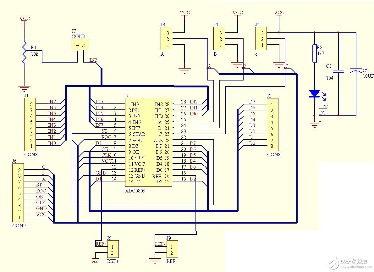
Figure 4-1: ADC0809 hardware circuit diagram
Easy Electronic Technology Co.,Ltd , https://www.yxpcelectronicgroups.com