With the rapid development of storage technology, storage capacity has increased rapidly, and the data transmission speed of storage systems has become a major bottleneck. Optical fiber transmission has its advantages in speed. However, fiber transmission is limited by Fibre Channel interfaces. Therefore, a key technical issue in the application of Fibre Channel to high-speed data transmission is the design of the interface. This paper effectively addresses high data transmission. The bottleneck at the interface has practical significance.
1 Scheme design
The complete implementation should include PC software programming, Virtex-5 development board bottom link implementation. The software compilation of the PC mainly implements link creation and cancellation control, data framing, data transmission control, and display during transmission; the VirteX-5 development board mainly implements data link penetration and supports frames defined by the host computer. Structure transmission process.
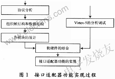
As shown in Figure 1, the implementation process of the interface adapter function mainly includes the correct understanding of the protocol, according to the organization of the frame structure and data structure of the protocol, the design and writing of the specific implementation module, and the integration of the VirteX-5 bottom link to achieve optical fiber communication Interface adapter function.
2 The specific realization of the design
2.1 Protocol analysis and tailoring
For different application environments, the FC protocol should be appropriately tailored, and the protocol standards should be used as efficiently as possible. FC protocol is a protocol system with five layers. Including: FC-0 layer, FC-1 layer, FC-2 layer, FC-3 layer, FC-4 layer.
The functions of each layer are:
(1): FC-O: mainly specifies the physical interface, including the transmission medium, transceiver and interface.
(2) FC-1: 8 B / 10 B encoding; serialization and deserialization; bit and word synchronization.
(3) FC-2 specifies the transmission mechanism of Fibre Channel:
Detection and identification of ordered sets; FC port state machine; frame transmission and reception, validity check when frame reception; flow control; frame management; exchange and sequence management; data frame and response; multicast and broadcast; sub Segmentation and reorganization; error detection and recovery.
(4) FC-3: basic link service; extended link service; query group.
(5) FC-4: Map the upper layer protocol. This article mainly maps the MILstd-1553B protocol.
2.2 Code design of each module in software programming
The design part of software implementation: GUI module design, device abstraction layer design, task processing module design, FC protocol and physical function module design.
(1) The GUI part is mainly used for display, and related parameters of the interface adapter can be set and displayed on the interface. GUI module design content includes: overall interface, link parameter area, link establishment area, information display area.
(2) Design of device abstraction layer. This part is to shield the differences between different physical devices in the lower layer; provide a simpler way to make the upper module communicate with the logic. This layer needs to provide the device operation interface supported by the upper layer and the function interface provided by encapsulating the WinDriver driver internally to realize the function support of the upper layer.
(3) Design of task processing module. Mainly realize the different task operation conditions of the link and data. The link data area and the file data area need to save their respective task data and status. In addition, it is the basis for the GUI module to change the LIST, so that it also needs to save the status and data possessed by the lower layer protocol.
(4) Design of FC protocol and physical function module. This part mainly describes the task sending protocol and link establishment protocol.
â‘ Registration process of link establishment: Before data transmission, it is necessary to establish a link between the sending end and the receiving end through registration. First, the sending end embeds the information such as the address ID to be registered in the frame information, and sends the frame information to the receiving end; then, after receiving the frame information, the receiving end interprets the relevant information. If the frame integrity check is met, then Establish a link at both ends. If the relevant inspection is not satisfied, the registration process is terminated.
â‘¡The process of canceling the link: when the link needs to be cancelled, first, the sender embeds the information such as the address ID to be cancelled into the frame information, and sends the frame information to the receiver; then, after receiving the frame information, the receiver interprets it If the relevant information meets the check of the integrity of the frame, the two ends log out the link, and if the related check is not met, the logout process is terminated.
â‘¢Data transmission process: Data transmission is the fundamental purpose of link establishment. The simplified data transmission process is shown in Figure 2.

2.3 The bottom guarantee of the Virtex-5 development board
(1) The system construction logic design mainly completes the following functions:
Control PCIE hard core to interact with upper layer software; add CRC check to upper layer transmission data; complete FC link initialization process; complete FC flow control function; complete FC-2 error processing; control ROCKET I / O to pass upper layer software data through ROCKET I / O sending; control ROCKET and I / O to transmit the received and recovered data to the upper layer software.
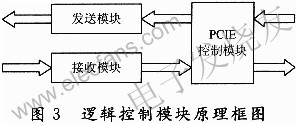
(2) The logical design module composition: the bottom logic control module mainly completes the FC physical layer communication, which mainly includes three parts: the sending module, the receiving module and the PCIE control module, each module is divided into multiple sub-modules according to different functions, and is controlled in PCIE In the module, there are some buffers to store the data transmitted by the receiving module and the corresponding data information, and the sending module will also read the data from the cache of the PCIE control module and transmit it. The functional block diagram is shown in Figure 3.
Data transmission module This module sends different information by reading the status information of the host computer. When ACK is enabled, the module sends ACK. When the data is enabled, the module sends a fixed number of frames of data. The data sent is Read from cache, CRC is added by this module. IDLE code is sent when idle.
The data receiving module receiving module includes a receiving control module, a CRC module and a temporary buffer module. Mainly complete the reception of data and link control frames and preparation signals, and implement CRC check, judge different types of data frames or control frames according to the frame header, and store them in the cache, and put the relevant information of the frame into the corresponding In the cache.
PCIE interface control module This module mainly decodes into the corresponding enable according to the value of the register on the PCIE bus address, writes the data on the PCIE bus to the corresponding data, sends buf-f, and ACK sends the buff. Yes, it can be decoded into the corresponding register value of the corresponding address on the corresponding PCIE bus, and the buffACK data received by the data reception is written into the corresponding PCIE address.
2.4 Final realization
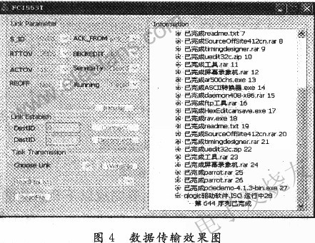
Through the combination of the host computer and the FPGA development board, the high speed of the fiber channel interface adapter is realized. The transmission effect diagram is shown in Figure 4.
3 Conclusion
Through the combination of the host computer and the FPGA development board, the design of the interface of the fiber channel in the high-speed data transmission process is simulated and realized. Although the design is implemented in the form of a host computer and an FPGA, only in terms of design ideas, it has certain reference significance for the actual development of Fibre Channel interface adapters.
Welcome to reprint, this article comes to the electronic enthusiast network (http: //)
Festoon bulbs are usually be used as interior lights, trunk light, glove compartment lights and license plate lights. There are many different types of interior bulb. Interior lights for indoor lighting are usually installed in the center of the car interior. It's better to light up the car interior evenly. The trunk light is a humanized device. When the lid is opened, a light is automatically lit in the luggage compartment to make it easy to pick up. Glove compartment lights is usually be installed in front of the front passenger side small storage space. Licence plate bulb illuminate sign on a vehicle that shows its registration number. License plate lamp is at night or when the sky is dark and wide light open together to light the lamp, according to the relevant provisions of the licence, all vehicles when driving at night, must be open after the car license plate lamp.
Auto Festoon Bulb
Auto Festoon Bulb,LED Light Dome Bulb,Auto Lighting System,Car LED Bulb
Heshan Jianhao Lighting Industrial Co., Ltd. , https://www.sunclubtw.com