introduction
As the sensor changes from a single to an array structure in the past, the signal to be processed by the instrument also changes from a single parameter signal to a complex image signal. At the same time, the acquisition and processing of the signal becomes more and more complicated. Array acoustic wave signal acquisition and processing system, and then developed an array sonic logging tool, has become an urgent need for the development of China's petroleum logging instruments. To this end, a DSP-based array acoustic wave signal acquisition and processing system is designed. This system will be used as part of the array acoustic logging tool being developed for oilfield exploration.
System overall design
The array sonic tool consists of a sound system, an electronic circuit, and a steel casing. At the lowest end, the sound system consists of a transmitting crystal that emits sound waves and a sensor array that receives sound waves and converts them into electrical signals. The electronic circuit is divided into a power supply module, a main CPU module, and an acquisition module. Among them, the main CPU module is the control part of the array sonic logging tool, which transmits the parameters of the ground part to the acquisition module and the sound system to the acquisition module and the sound system on the one hand, and transmits the data transmitted from the acquisition module to the other hand on the other hand. Ground part. The acquisition module is an array sound wave acquisition and processing system. One end is connected to the sensor array of the sound system, and the other end is connected to the main CPU. The main function is to sample, digitize and carry out the signals transmitted from the front-end sensor array under the control of the main CPU. The processing of the series, and then upload the processing results to the main CPU.
According to the performance requirements and reliability and low-power design principles of the array acoustic wave acquisition and processing system, the design decided to adopt an eight-channel implementation scheme with a DSP chip as the core, as shown in Figure 1. Since the data signal sent by the front-end sensor array is relatively weak, the amplifier must first amplify the signal, and the amplifier can effectively attenuate or eliminate the influence of the back-end ADC on the front-end analog sound input signal. The amplifier is followed by an ADC that forms a channel for acquisition and processing from the amplifier to the DSP. There are eight such channels in the system. The CPLD in Figure 1 is the control logic part of the system. In addition, considering the system reliability and real-time requirements, the system is designed to have one DSP processor per channel instead of eight channels sharing one DSP processor.

Figure 1 Schematic diagram of the overall structure of the array acoustic wave signal acquisition and processing system
DSP design
DSP chip
Since the other chips of the entire array sonic logging tool are powered by +5V, the array acoustic wave acquisition and processing system is used as part of the logging tool. If the selected DSP chip is not powered by +5V, the power conversion chip is required for voltage conversion. This not only complicates the circuit, but also degrades system performance. Therefore, this design selected TI's DSP chip - TMS320C542 (hereinafter referred to as C542).
In addition to the general advantages of TMS320C54x, C542 has a single-cycle fixed-point instruction execution time of 25ns, a relatively high running speed, and can complete the system acquisition and processing functions; it also has a BSP automatic buffer serial port and a TDM time-division multiplex port. Both can be used as SP standard synchronous serial ports. In addition, both the core and I/O pins operate at +5V, so no voltage conversion chip is required for use.
Bootstrap loading design
The bootload of the traditional DSP system program code mostly uses the parallel EPROM as the memory mode of the application. The biggest drawback is that the EPROM does not support online erasing, which brings great inconvenience to the debugging of the system, especially for the surface mount package. Memory, this method is basically not available.
In the design of the system, FLASH which can be erased online is used instead of EPROM as the memory of the program code. Therefore, it fundamentally overcomes the inconvenience caused by the traditional method in system debugging, and is particularly suitable for the memory of the surface mount package. During the debugging process, the program code is directly written into the FLASH through C542. After power-on, the C542 can perform the bootloader operation according to the FLASH mode, which greatly reduces the difficulty of debugging the hardware system.
This system uses 8-bit parallel loading. Check if the MP/MC pin is low during C542 reset. If not, execute the user program from the external program memory 0FF80h; if yes, execute the program from 0FF80h of the on-chip ROM. When starting the manufacturer's bootstrap loader program in ROM, it should first be initialized and then check the INT2 pin. If it is valid, it will be loaded from HPI-RAM. If it is invalid, the I/O port strobe signal IS will be Low level, the bootloader selection word (BRS) is read from the I/O port at address 0FFFFh. The lower 8 bits of BRS determine the way of bootstrap loading. If the lower 2 bits of BRS are 01, then 8 bits are loaded in parallel, and then the bootstrap loader can be based on the FLASH address (high 6 bits in BRS + 0000000000). Read the bootstrap table. After the bootloader sends all the program code in the FLASH to the program memory, it immediately transfers to the destination address and starts executing the program code.
In this design, the FLASH chip is selected by AMD's Am29F010, which has a capacity of 1 Mbit. Because the C542 can only address 64K addresses, the A16 pin of the Am29F010 is grounded.
The hardware design of the DSP online loading system is shown in Figure 2. The DS is not directly connected to the CE at the time of design, but the A14 and A15 are respectively connected to a non-gate. The output terminals of the two non-gates are connected to the IS together with the IS. The output of the OR gate is connected with the DS. An AND gate, the output of the AND gate is connected to the CE. This design makes the 48K to 64K address space of the Am29F010 a data and I/O multiplex space. During the bootloader load, the bootloader selection bit can be read from the I/O port of the Am29F010 address 0FFFFh.
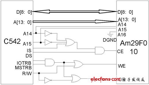
Figure 2 DSP online loading hardware design
Trench Cover,Trench Drain,Drain Cover,Steel Trench Covers
Hunan Furui Mechanical and Electrical Equipment Manufacturing Co., Ltd. , https://www.frcornthresher.com