Discuss the causes of radiation emissions
Detailed description of the process of solving the high-frequency circuit radiation emission exceeding the standard
solution:Stop the IF board and eliminate the possibility of interference from the IF board
Use SDRAM_CLK0 as the SDRAM operating clock
Solving the problem of excessive emission of radiation by using off interference sources and reducing the amplitude of high-frequency current
statement of problem
The development of communication technology requires the speed of the device to become higher and higher, and the electromagnetic compatibility problem caused by this is more serious. This paper takes the terminal subscriber unit (SU) of the wireless broadband access system as an example to explore the problem of excessive emission of communication products.
The end user unit of the wireless broadband access system consists of 860 small system, 8240 small system, FPGA (field programmable gate array) and baseband intermediate frequency unit, of which 860 small system, 8240 small system and FPGA circuit are on one PCB (printed circuit board) On, called the network interface board; the baseband IF circuit is a single PCB, called the baseband IF board. The two are connected through a socket to transmit signals and power. The outer casing of the device is an injection molded case, and the inner layer is not sprayed with conductive paint. The author tested the radiation emission index of the product.
The test environment is an anechoic chamber. The test equipment is a wideband antenna, spectrum analyzer and signal amplifier. The antenna can be lifted and lowered within a height of 1 m and 4 m. The product to be tested is placed on a 360° rotating platform, 3 m from the antenna. . When the measurement is rotated, the lifting antenna finds the maximum interference, and the antenna measurement takes both horizontal and vertical polarization.
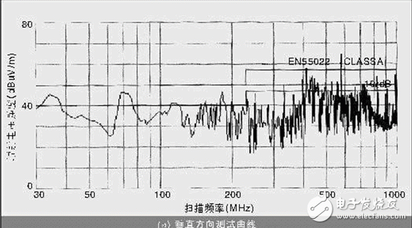
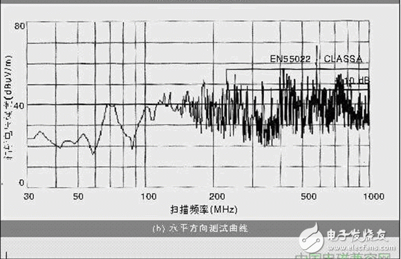

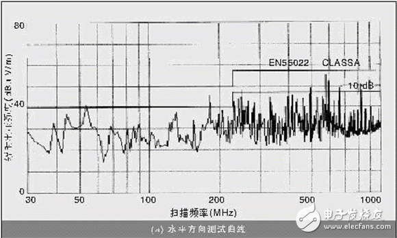
According to the electromagnetic compatibility (EMC) test requirements of the access equipment, the equipment is powered up normally, and the test equipment is scanned in the frequency range of 30 to 1 000 MHz, where electromagnetic interference (EMI) is required in the frequency range of 30 to 230 MHz. The quasi-peak is below 40 dBuV/m, and the quasi-peak of EMI is below 47 dBuV/m over the 230-1000 MHz frequency range. The result of the test is: in the vertical direction, the standard exceeds 4.08 dB at 412.5 MHz, and exceeds 3.5 dB at 577.5 MHz; in the horizontal direction, it exceeds 7.9 dB at 577.5 MHz, see Figure 1.
Considering that there is a modulation and demodulation circuit on the IF board, the carrier frequency is relatively high (349 MHz). For this reason, the 5 V and 3.3 V operating power of the IF board is disconnected, so that the IF board stops working. When the electromagnetic interference of the device is tested again, there is still an excess of the above two frequency points, so that the possibility of the above-mentioned frequency interference can be eliminated by the intermediate frequency board.
Cause AnalysisAny electromagnetic compatibility problem consists of three elements, namely the interference source, the sensitive source and the coupling path. If one of the three elements is missing, the electromagnetic compatibility problem will not exist. Therefore, when solving the electromagnetic compatibility problem, we must start from the analysis of these three elements, and then take appropriate measures to eliminate one of them according to the specific situation.
Start with the analysis of the source of interference. In communication products, the operating clock of the circuit is getting higher and higher, and the rising/falling edge of the signal is getting steeper and steeper, and the electromagnetic compatibility problem caused by this is becoming more and more acute. The electromagnetic compatibility design of digital circuits is to consider the frequency bandwidth determined by the rising and falling edges of the digital pulse, not the repetition frequency of the digital pulse. According to the empirical formula, the formula for calculating the EMI emission bandwidth can be expressed as:
f=0.35/Tr (1)
Where f is the frequency (in GHz) and Tr is the signal rise/fall time (in ns). It is not difficult to see that a clock signal with a rising edge of 2 ns has a bandwidth of up to 160 MHz and a radiation bandwidth of up to 10 times, or 1.6 GHz.
In electrical engineering, periodic currents, voltages, signals, etc. can be represented by a periodic signal, ie f(t) = f(t + kT), where T is the period of the periodic function. If a given periodic function satisfies the Dirich's condition at the same time, it can be expanded into a Fourier series:
The first item A0 is called the DC component, the second term is called the first harmonic (or the fundamental component), and the other items are collectively referred to as the higher harmonics, that is, 2, 3, 4 times... kth harmonic . An ideal square wave signal contains a rich harmonic component. In practical digital circuits, the square wave is not ideal, it has a certain rise and fall time. The attenuation rate of the square wave spectral envelope is not only related to the frequency of the square wave, but also to the duration of the square wave pulse. The shorter the duration of the square wave pulse, the greater the interference amplitude of the higher harmonics.
Since there are no frequency signals of 412.5 MHz and 577.5 MHz on the terminal network interface board, it is suspected that these two frequencies may be harmonic components of some frequency signals. In high speed circuits, the clock current is the first source of radiation. The author has performed statistics on each clock signal on the terminal network interface board, as shown in Table 1.
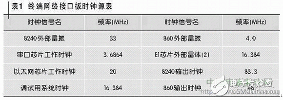
By rough calculation, the 412.5 MHz signal is approximately equal to the 5th harmonic of 83.3 MHz (83.3 & TImes; 5 = 416.5 MHz), while 577.5 MHz is approximately equal to the 7th harmonic of 83.3 MHz (83.3 & TImes; 7 = 583.1 MHz).
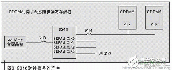
Figure 2 shows the generation of the 8240 clock signal. The 8240 external active crystal oscillator generates an oscillation frequency of 33 MHz and is sent to the 8240 chip. It is phase-locked by an internal PLL (phase-locked loop) and outputs 83.3 MHz frequency. It is used as the operating clock of SDRAM (Synchronous Dynamic Random Read-Write Memory), 8240. There are 4 pins that can simultaneously send the 83.3 MHz clock: SDRAM_CLK0 to SDRAM_CLK3, and the switch can be set in the 8240 internal register. In the circuit design, the SDRAM_CLK0 is used as the SDRAM working clock, and the other SDRAM_CLK3 is sent to a test point to facilitate the measurement of the clock signal during debugging. The other two channels are set to the off state, and the clock is not outputted externally.
Preliminary testIn order to confirm that the two interference frequencies of 412.5 MHz and 577.5 MHz are caused by the 83.3 MHz clock, I first try to cancel the 8240 PLL configuration circuit, that is, the 8240 phase-locked loop does not work, and does not output the 83.3 MHz clock, and then enters the anechoic chamber. test. It was found that there was no over-frequency point in the scanning band of 30 to 1 000 MHz, and the obtained test curves were below the quasi-peak value specified by the standard. Therefore, it can be judged that the interference source is the 83.3 MHz clock signal of the 8240 output.
Although the interference source is located, the 83.3 MHz clock must be output in the actual application. The next question is how to solve the EMI problem caused by the 83.3 MHz clock. Because the structural scheme of the circuit has been determined, it is too difficult to remove the sensitive source, so the focus is to find the interference coupling path.
In communication products, the root of radiation is usually in its digital circuit part, and the radiation of digital circuits can be divided into differential mode radiation and common mode radiation according to its mode: differential mode radiation is caused by current flowing through the wire loop in the circuit. These loops are equivalent to small antennas that are working, radiating magnetic fields into space, differential mode radiation is proportional to loop current and loop area, and proportional to the square of the current frequency; common mode radiation is due to the presence of undesired voltages in the circuit. As a result, this voltage drop causes some parts of the system to be at a high potential common mode voltage, and the signal lines on the PCB are excited by the common mode voltage to form the antenna radiation and frequency, antenna length and flow of the radiated electric field. The amplitude of the common mode current through the antenna is proportional.
SolutionAfter understanding the mechanism of radiation emission, the following measures can be taken to solve:
a. Turn off the interference source
There is a test hole on the surface of the board, which is the SDRAM_CLK3 signal in Figure 2, with a frequency of 83.3 MHz, used as a measurement clock signal during debugging. Because the signal is in an unloaded form and the frequency is relatively high, it can be physically equivalent to an antenna, radiating high frequency electromagnetic waves into space, which contains higher harmonics of 83.3 MHz.
The author modified the 8240 control register, shielded the SDRAM_CLK3 signal, and did not output the 83.3 MHz clock. The EMI test was performed again. As a result, 577.5 MHz did not exceed the standard in the vertical and horizontal directions, and 412.5 MHz had a margin of 3.85 dB in the vertical direction. The direction has a margin of 0.25 dB. This shows that the radiation effect of the test point is still very strong, and it is also effective to turn off the test point. (2) Reduce ground noise.
The precondition for the above test results is that the baseband IF board is not powered. In practical applications, the IF board should also be in working condition. After restoring power to the IF board, the test results changed immediately: the 412.5 MHz point exceeded the standard by 4.21 dB in the horizontal direction and exceeded the standard by 4.51 dB in the vertical direction; while the 577.5 MHz exceeded the standard by 5 dB in the horizontal direction, and the vertical direction did not exceed the standard.
The IF board was tested separately, and the above two over-standard frequencies were not found. Using the DC voltage regulator to test the board, there is still interference at these 2 points, which eliminates the possibility of interference caused by the power supply unit. This phenomenon shows that with the operation of the IF board, the operating current of the power supply increases, the common mode interference caused by the ground noise increases, and the harmonics of 83.3 MHz increase the radiation intensity through the ground noise.
The author used a high-speed oscilloscope to measure the working ground noise (Vp-p) of the network interface board to be 96 mV. After the IF board works, the noise increases to more than 130 mV. This measurement method may have deviations, but the overall trend is that after two boards are working at the same time, it does increase the ground noise, which has a certain impact on EMI, but the impact is limited.
In the PCB layout, the author has considered the EMI problem of the high-speed signal line, so some key signal lines, high-speed clock lines are wired inside the PCB, sandwiched between the power layer and the ground layer, it should be said that the shielding measures are relatively reliable. Further, it is also conceivable to adopt a "package" method on both sides of the 83.3 MHz clock line, and wrap the clock line with two parallel ground lines to reduce EMI emission to some extent.
b. Reduce the amplitude of the high frequency current
In high-speed circuits, parasitic resistance, parasitic capacitance, and parasitic inductance are present on the PCB lines and integrated circuit pins to different degrees. Different impedance characteristics are presented at different frequencies. From the perspective of signal integrity, series impedance Matching is effective in suppressing signal reflections and oscillations, which are the main sources of EMI.
Does the 83.3 MHz clock line cause EMI over-standard due to improper line impedance matching and signal reflection on the line? In the design stage of the board, I used Cadence's SI (Signal Integrity) simulation tool Signal Explore to perform a detailed simulation of the series matching resistors of the key signals. The 51R matching resistor was selected to better suppress the clock signal. Punching and oscillating to minimize EMI emission intensity. Selecting a matching resistor with a larger resistance value can make the signal over-punching to be lower, and the EMI emission will also be improved. However, this will cause the rising/falling edge of the signal to slow down. In severe cases, the system timing will be wrong. A series of SI issues. Therefore, the choice of matching resistors should be adequate, taking into account the dual needs of signal quality and timing.
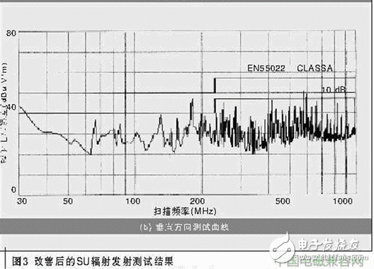
At this point, there is no better way to improve the circuit design. With the assistance of the structural engineer, the inner surface of the injection molded case used in the terminal unit is sprayed with conductive paint to shield the radiated electromagnetic waves, and the network interface board and the baseband intermediate frequency board are all powered up. The results of the retest are shown in Fig. 3. As can be seen from Figure 3, in the frequency band of 30 to 1 000 MHz, there is no over-frequency point. The 412.5 MHz that I am most concerned about has a margin of 10.49 dB in the vertical direction and 577.5 MHz has a margin of 6.9 dB in the vertical direction. It can be seen that there is a 2.1 dB margin in the horizontal direction, and the shielding effect is better than expected. According to experience, the signal attenuation before and after spraying conductive paint is generally 2 to 3 dB, and the result of this test is reduced by nearly 10 dB!
in conclusionThe author has been responsible for the electromagnetic compatibility performance test of communication products and researched the corresponding solutions. He has conducted a number of electromagnetic compatibility tests on the terminal network access unit and the base station access unit. Among all the test items, the most difficult and difficult to solve is the problem that the radiation emission index exceeds the standard.
One of the difficulties is to find sources of interference. Most of them come from the higher harmonics of high-speed clock signals, especially the odd-order harmonics: 3, 5, 7, and 9 times, as mentioned in this article, the 5th and 7th harmonics. At the same time, it is necessary to exclude the interference of other components. For example, the author tests the IF board and the power supply unit separately, and eliminates them one by one, and finally locates the interference source on the 83.3 MHz clock source.
The second difficulty is that after the interference source is located, the countermeasures are difficult to select. First, from the mechanism of radiation generation, look for signal lines that are most likely to produce antenna effects, such as the surface test holes described herein. The most effective way is to cut off the radiation path so that it does not become a good transmitting antenna.
Signal reflection and oscillation caused by improper impedance matching of signal lines are also important causes of EMI. The best method is to perform strict and detailed simulation of the signal at the design stage, which is first solved from the perspective of signal integrity.
It is best to minimize EMI from the aspect of circuit design. In the case of powerlessness, we should consider starting from the structural process and increase the shielding measures. The effect of suppressing EMI on the inner surface of the injection molded case is Obvious.
Ningbo Autrends International Trade Co.,Ltd. , https://www.supervapebar.com