This article is to explore the application and design of audio systems in mobile phones and PDAs, so that systems and developers can design products that are suitable for consumers.
This article refers to the address: http://
Wireless portable electronic product considerations
The main factors that must be considered when selecting an audio power amplifier are listed below.
Higher Power Supply Rejection Ration (PSRR)
The audio power amplifier must have a high PSRR to avoid interference from power and wiring noise.
Fast turn on & off
With a long standby time, the basic appeal of mobile phones or PDAs, Class AB audio amplifiers are about 50 to 60% efficient, and Class D audio amplifiers are 85 to 90% efficient, regardless of the audio amplifier used, to save The power consumption needs to enter the standby state when the audio amplifier is not needed. However, when a sound occurs, the audio amplifier must immediately enter the power-on state.
No "Switch & Pop" sound
The "switching noise" sound often occurs when the audio amplifier enters the switch, or when it returns to normal state from standby, even when the 217Hz mobile phone communication signal, the user of the mobile phone or PDA will never want to hear disturbing noise. It is an important requirement to add the "switching switching noise" cancellation circuit to the audio amplifier.
Lower operating voltage
In order to extend battery life, it is still required to work at temperatures as low as 1.8 volts.
Low current consumption and high efficiency
Using a CMOS process IC reduces current consumption and sometimes requires a Class D audio amplifier to extend the operating time of a mobile phone or personal digital processor.
High output power
It has a higher output power at the same operating voltage, that is, the closer the swing of the output signal is to Vcc and GND, the higher the output power.
Smaller package (Micro SMD)
The shrinking appearance of mobile phones or personal digital processors has made IC packaging technology more and more important, and Micro SMD is the packaging technology that is more commonly used today.
Output power calculation
The single-ended amplifier has the gain as shown in (Figure 1): (Formula 1) Gain = Rf / Ri Rf: Feedback Impedance Ri: Input Impedance
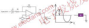
(Figure 1) Single-End (Single-end) Amplifier
The output power = (VRMS) 2 / Rload, VRMS = Vpeak /2 1/2, so the single-ended (Single-end) amplifier output power = (Vpeak) 2 / 2Rload. The bridged (BTL) amplifier, as shown in (Figure 2), consists of two single-ended amplifiers with a phase difference of 180°, so the gain is (Equation 2) Gain=2Rf/Ri Rf: feedback impedance Ri: Input impedance is output power = (VRMS) 2 / Rload, bridged VRMS = 2Vpeak / 21/2, so bridge output power = 2 (Vpeak) 2 / Rload = 4 × terminal amplifier output power.
Figure 2) Bridge amplifier and waveform applied to the positive and negative terminals of the horn
Input and output coupling capacitor value selection
As shown in Figure 1, the input impedance and the input coupling capacitor form a high-pass filter. To obtain a lower frequency response, a larger capacitance value needs to be selected. The relationship can be expressed by the following formula: (Formula 3) fC = 1/2 ∠(RI) (CI) fC: High Pass Filter Cutoff Frequency RI: Input Impedance CI: Input Coupling Capacitor value that blocks the DC voltage and couples the input signal to the input of the amplifier.
In mobile communication systems, due to volume limitations, even with large input coupling capacitance values, the speaker typically does not exhibit a frequency response below 50 Hz. Therefore, assuming an input impedance of 20K ohms, only the input coupling capacitance value is greater than 0.19uF. In this case, 0.22uF is the most appropriate choice.
For the setting of the output coupling capacitance value, as in Figure 1, if you want to get a better frequency response, the capacitance value also needs to choose a larger capacitance value. The relationship can be expressed by the following formula: (Formula 4) fC =1 /2âˆ(RL)(CO) fC: high-pass filter cut-off frequency RL: impedance of the speaker (headphone) C output coupling capacitor value
For example, when using a 32 ohm earphone, if you want a 50Hz frequency response, you need to choose an output coupling capacitor value of 99uF. In this case, 100uF is the most appropriate choice.
Thermal considerations
When designing a single-ended amplifier or a bridged (BTL) amplifier, power consumption is one of the main considerations. As the output power is increased to the load, the internal power consumption is also increased.
The power consumption of a bridged (BTL) amplifier can be expressed by the following equation: (Equation 5) PDMAX_BTL = 4 (VDD) 2 / (2 ∠2 RL) VDD: Supply voltage RL: load impedance applied to the bridge (BTL) amplifier
For example, when VDD = 5V, RL = 8ohm, the power consumption of the bridge amplifier is 634mW. If the load impedance is changed to 32ohm, its internal power consumption is reduced to 158mW.
The power consumption of a single-ended amplifier can be expressed by the following equation: (Formula 6) PDMAX_SE=(VDD)2/(2âˆ2RL) VDD: Supply voltage applied to a single-ended amplifier RL: The load impedance, ie the power consumption of a single-ended amplifier, is only a quarter of that of a bridge amplifier. All power consumption is added up by the thermal resistance of the IC (?JA) which is the temperature rise.
Layout considerations
Designers are online, and some basic guidelines must be followed, such as:
All signal lines are grounded as single point as possible;
In order to avoid interference between the two signals, parallel routing should be avoided, and the 90° crossover method should be adopted.
The digital power supply and grounding should be separated from the analog power supply and grounding.
The high-speed digital signal trace should be kept away from the analog signal trace and should not be placed under the analog component.
3D enhanced stereo in mobile phones and PDA applications
As far as most people know, "3D sound" is neither mono nor dual channel. It is an audio processing technology that allows listeners to feel the location of sound in an unrealistic environment. It is necessary to pay great attention to the placement and number of speakers (horns). However, in mobile phones and PDA processors, it is impossible to place so many speakers. Therefore, it has been developed to simulate "3D sound effects" by using two speakers plus hardware or software, which is called "3D enhanced stereo sound effect" ( 3D Enhancement). (Figure 3) is a 3D enhanced stereo audio frequency system block diagram for stereo phones or personal digital processors. This audio frequency system consists of the following parts:
Post-amplifier: Includes a stereo speaker (horn) driver, a stereo headphone driver, a mono earphone amplifier (earpiece), and a line out for hands-free handsets, such as a car's hands-free handset Output.
Volume control: Volume control is available in 32 levels, and the volume of the left, right and mono can be controlled independently.
Mixer: Used to select the relationship between the output and the input source. It can transmit and mix stereo and mono inputs, and divide these inputs into 16 different output modes, enabling system designers to flexibly transmit and mix singles. Channel and stereo audio signals, no limit to the signal can only be transmitted to stereo speakers or stereo headphones.
Power control and "switching noise" elimination circuit.
3D enhanced stereo, in hardware.
Use the I2C compatible interface to control the functionality of the chip.
Sound in different positions
When passed to the left and right ears, different phase differences will occur. Using this phase difference principle and hardware method, you can simulate 3D enhanced stereo sound. Even if the system is limited in size or equipment, you must improve the positioning of the high and low parts of the stereo when the left and right speakers must be placed very close. Various problems.
As shown in Figure 3, the 3D enhanced stereo block diagram shows an external resistor and capacitor circuit to control the sound of the 3D enhanced stereo. Two separate resistor and capacitor circuits are used to control the stereo speakers and stereo headphones. 3D enhanced stereo effect.
In this resistor and capacitor circuit, the "quantity" of the 3D enhanced stereo effect is set by the R3D resistor and is inversely proportional. The C3D capacitor is used to set the 3dB low frequency cutoff frequency of the 3D enhanced stereo effect at the low frequency cutoff frequency. The 3D enhanced stereo effect can be seen above, and increasing the C3D capacitance value will lower the low frequency cutoff frequency, and the relationship can be expressed by the following formula. (Formula 7) f3D(-3dB)=1/2âˆ(R3D)(C3D)
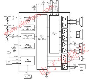
(Figure 3) 3D Enhanced Stereo Audio Subsystem Block Diagram
in conclusion
Since mobile phones and personal digital processors have evolved into multi-functional portable devices that offer a variety of different entertainments, manufacturers have tried to use high-quality audio systems and long-life batteries, and to make such portable electronic devices The product features a stereo speaker amplifier, a variety of different mixing, and 3D enhanced stereo, while also being as thin and light as possible. However, its design scope still does not deviate from the above basic principles, which is another purpose to be expressed in this article.
Silicone Thermal Conductive Gap Filler Pad could reach 6.0 W/mk Between heat-generation Component and heatsink Automotive engine control, Graphices Cards, Telecom device Wireless Hub,Military equipment, power supply Cooling Module, Thermal module,
1. High bond strength to surfaces
2. Thermal conductivity in combination with electrical isolation
3. Excellent wet out
4. High temperature stability
Application:
1.For CPU, LED,PPR heat sink, microprocessor
2.For any power consumption semiconductor
2.Replacing screws, fasteners and other fixed means
4.Fixing heat sink on the power supply circuit board
5.Fixing heat sink on vehicle control circuit board
6.Fixing heat sink on packaged chips
we could die cut any size and shapes as customer design.


TP-600
TEST ITEM
TEST MOTHOD
UNIT
VALUE
SIZE
mm
400*200MM
COLOR
Visual
Blue
THICKNESS
ASTM D374
mm
0.3-10MM
GRAVITY
ASTM D792
g/cc
2.85±0.1
HARDNESS
ASTM D2240
Shore 00
25±5
TENSILE STRENGTH
ASTM D412
kg/cm2
55
ELONGATION
ASTM D412
%
60 95
TEMP
EN344
℃
-40~+220
VOLUME RESISTIVITY
ASTM D257
Ω•CM
3.1*1011
BREAKDOWN VOLTAGE
ASTM D149
kv/mm
5
VOLUME IMPENDENCE
ASTM D257
Ω.cm
1.7×10¹³
Weight Damnify
200℃ 200H
%
≤1
Thermal Resistance
ASTM D5740
℃/ W
0.18
FLAMMABLITY
UL-94
V-0
THERMAL CONDUCTIVITY
ASTM D5470
w/(m•k)
6
TP-240
TEST ITEM
TEST MOTHOD
UNIT
VALUE
COLOR
Visual
GRAY
THICKNESS
ASTM D374
mm
0.5~10
GRAVITY
ASTM D792
g/cc
1.8-2.2
HARDNESS
ASTM D2240
Shore00
30±5
TENSILE STRENGTH
ASTM D412
kg/cm2
2.3
TEMP
EN344
℃
-40~+220
VOLUME RESISTIVITY
ASTM D257
Ω•CM
1.7*1013
BREAKDOWN VOLTAGE
ASTM D149
kv/mm
4
FLAMMABLITY
UL-94
V-0
THERMAL CONDUCTIVITY
ASTM D5470
w/(m•k)
2.4
Fiber glass reinforced
Test Item
Unit
Data
Test Method
Color
-----
gray\pink
Visual
Reinforcement Carrier
fiber glass
Thickness
mm
0.23\0.3\0.45mm±0.05
ASTM
D374
Spec
mm
300mm×50M
ASTM
D1204
Density
g/cc
1.7±0.1
ASTM
D792
Hardness
Shore 00
75±5
ASTM
D2240
Tensile Strength
kg/cm2
>180
ASTM
D412
pa
1.8*1011
ASTM
D412
Breakdown Voltage
Kv/mm
≥4.0
ASTM
D149
Volume Impedance
Ω.cm
1.7×10¹³
ASTM
D257
Continuous Use Temp
℃
-40~220
EN344
Thermal Resistance
℃/ W
0.25
ASTM
D5740
Flame Rating
------
V-0
UL
94
Thermal Conductivity
W/m.k
1.0
ASTM
E 1461-01
Thermal Conductive Pad
Thermal Conductive Pad,Thermal Pad Material,Thermal Interface Pad,Thermal Conductive Gap Pad
JINAN EMI SHIELDING TECHNOLOGY CO., LTD. , http://www.emirfi.com