Refueling version x47b exposure _x47b drone parameters
As a transformer engineer, mastering the necessary skills is essential before you can effectively contribute to the work chain. First and foremost, it's crucial to understand the role of the transformer within a circuit and to analyze the voltage and current waveforms that occur during operation. This foundational knowledge is key to developing innovative designs and troubleshooting issues that may arise during the transformer’s use.
In recent years, the development and application of power transformers have become more specialized. The design and manufacturing of low-power switching power supply transformers now align more closely with civilian needs. In this session, we will explore the design and production process of a low-power power transformer, providing engineers with practical insights and real-world examples.
**Detailed Design of a Switching Power Supply**
The first step in designing a switching power supply is to thoroughly review the specifications. While many engineers are familiar with this process, it's always beneficial to revisit and analyze them carefully. I'll guide you through the key considerations.
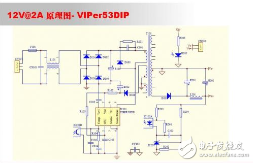
We’ll be focusing on a conventional isolated 12V 2A switching power supply that operates over a wide input voltage range.
**1. Determine the Power Requirements First**
Based on the specific application, an appropriate topology is selected. A flyback topology is often a good choice for such applications due to its simplicity and cost-effectiveness.
Note: I will use empirical formulas for calculations here. If needed, I can provide more detailed analysis and explanations.
**2. Selecting the PWM IC and MOSFET**
Once the flyback topology is decided, the next step is to choose the appropriate PWM IC and MOSFET for the initial schematic design. Whether you go for a discrete or integrated solution is up to you.
- **Discrete**: Using separate PWM ICs and MOSFETs allows for greater flexibility in power matching, but the design and debugging process tends to be longer.
- **Integrated**: These chips combine the PWM controller and MOSFET in one package, simplifying the design process and reducing development time. Ideal for beginners or projects requiring rapid prototyping.
**3. Creating the Schematic**
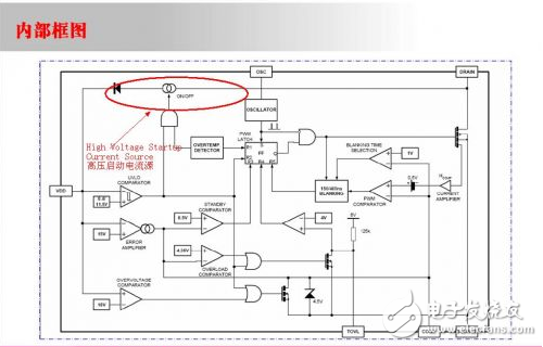
After selecting the components, the next step is to create the schematic. For this example, I've chosen the ST VIPer53DIP, which integrates the MOSFET. Why? Because it’s a reliable chip commonly used in our designs.
Before starting, it's important to review the datasheet and verify the basic parameters. Most datasheets include a sample schematic, which serves as a great reference for your design.
**4. Moving to PCB Layout**
Once the schematic is complete, the next step is to determine the component values and prepare for PCB layout. Different companies may follow different processes, so it's important to develop good design habits and adhere to the required standards.
This phase typically involves preliminary evaluation, schematic confirmation, and final sign-off before proceeding with calculations.
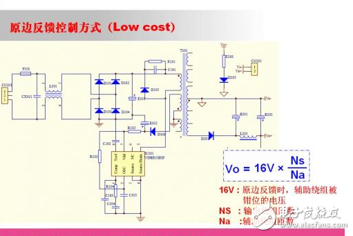
**Here is the corresponding schematic:**
Uv Curing Film For Mobile Tablet
Uv Curing Film For Mobile Tablet,Tempered Glass For Mobile,Phone Curve Edge Protector,Local Tempered Glass
Shenzhen TUOLI Electronic Technology Co., Ltd. , https://www.tlhydrogelprotector.com